Film-like composite structure and method of manufacture thereof

A structure and film-like technology, applied in semiconductor/solid-state device manufacturing, semiconductor devices, instruments, etc., can solve problems such as failure to obtain film structures

Inactive Publication Date: 2004-06-30
JAPAN SCI & TECH CORP
View PDF0 Cites 0 Cited by
  • Summary
  • Abstract
  • Description
  • Claims
  • Application Information

AI Technical Summary

Problems solved by technology

[0009] As mentioned above, the existing electronic components that utilize the Schottky barrier only utilize the overall Schottky barrier height of the metal-semiconductor interface, and fail to obtain the interface that makes the Schottky barrier different at the nanoscale. The membrane structure present in the region of

Method used


Image

  • Film-like composite structure and method of manufacture thereof
  • Film-like composite structure and method of manufacture thereof
  • Film-like composite structure and method of manufacture thereof

Examples


Embodiment 1

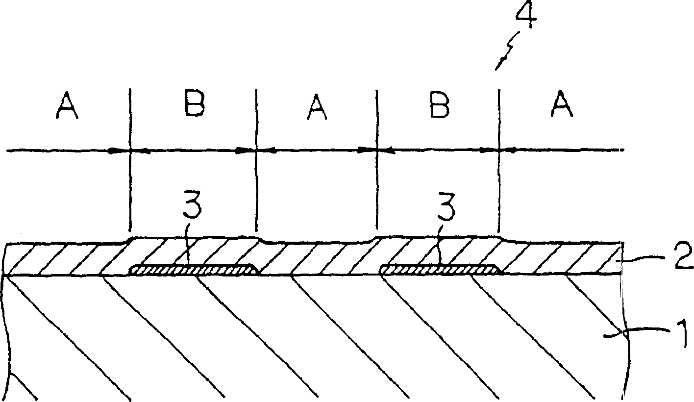
[0067] First, using a Si(111)·(7×7) substrate as the semiconductor layer 1, the size of the platform on the surface of the Si substrate is controlled to about 50nm. On the surface of a clean Si(111)·(7×7) substrate having such a mesa, first, an Au film with a thickness of 1 nm was formed by the MBE method while controlling the substrate temperature to 303K. Next, while controlling the substrate temperature to 303K, an Ag film with a thickness of 10 nm was formed by the MBE method. Here, an Au film is formed as the intermediate layer 3 , and an Ag film formed thereon serves as the metal layer 2 .

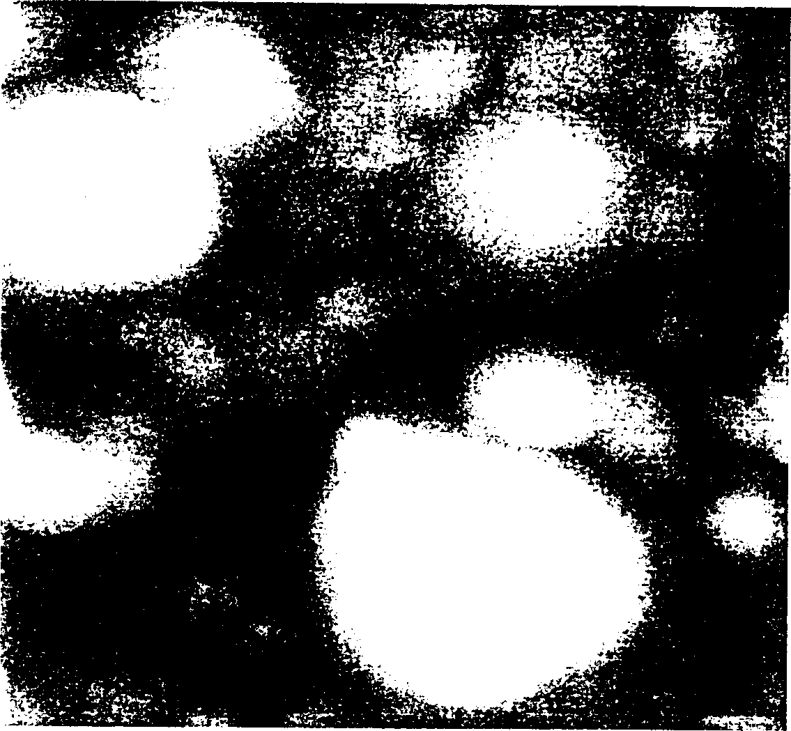
[0068] When performing STM observation and BEEM observation of such a composite film, it was confirmed that the Au film exists as an island on the platform, the region where Ag forms the interface with the Si substrate and the presence of an Au intermediate layer and the Au formation A region coexisting at the interface with the Si substrate. It was confirmed from the BEEM images ...

Embodiment 2

[0071] Using a Si(111)·(7×7) substrate as the semiconductor layer 1, on the surface of the cleaned Si(111)·(7×7) substrate, first, while controlling the substrate temperature to 973K, Formation of CaF as an insulator with a thickness of 1nm by the MBE method 2 membrane. The CaF 2 The membrane grows in bands from the steps. Secondly, the substrate temperature is controlled to 303K, and the CaF 2 The film was formed as an Au film with a thickness of 5.0 nm. Here, the CaF 2 A film is formed as the intermediate layer 3 , and the Au film formed thereon becomes the metal layer 2 .

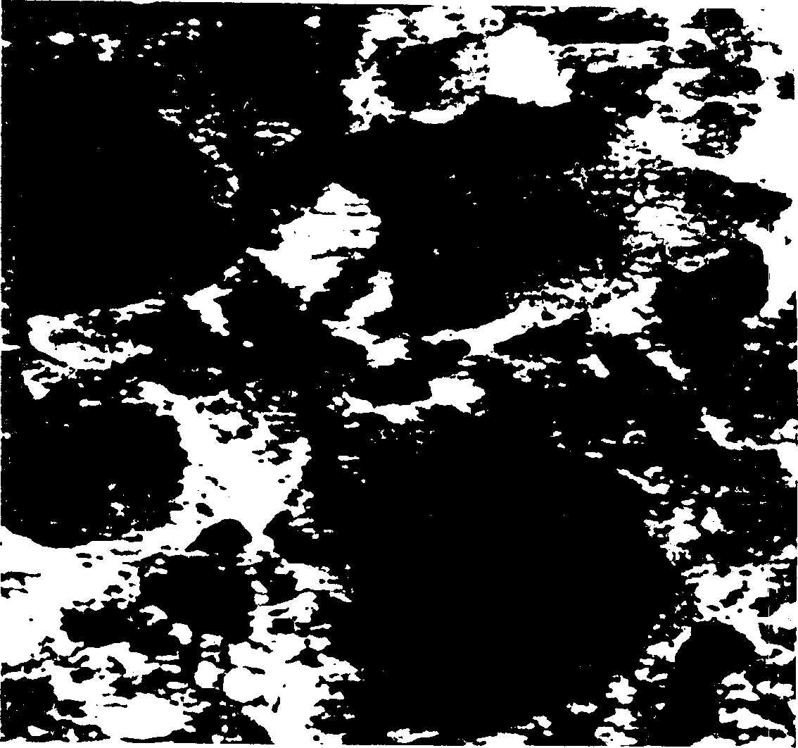
[0072] When STM observation and BEEM observation of such a composite film were performed, it was confirmed that the region where the Au film forms a direct interface with the Si substrate and the band-shaped CaF with a thickness of 1 nm 2 A region where the film intervenes at the Au-Si interface coexists. It was confirmed from the BEEM spectra of these regions that the Schottky barrier heights are...

Embodiment 3

[0074] A Si(111)·(7×7) substrate was used as the semiconductor layer 1, and the size of the mesa on the surface of the Si substrate was controlled to about 50 nm by oxidation treatment in the atmosphere and heat treatment in ultra-high vacuum. On the surface of a clean Si(111)·(7×7) substrate with such a platform, first, while controlling the substrate temperature to 773K, a CaF as an insulator with a thickness of 1 nm was formed by the MBE method. 2 membrane. Secondly, the substrate temperature is controlled to 303K, and the CaF 2 The film was formed as an Au film with a thickness of 5.0 nm. Here, the CaF 2 A film is formed as the intermediate layer 3 , and the Au film formed thereon becomes the metal layer 2 .

[0075] When performing STM observation and BEEM observation of such a composite film, it was confirmed that the CaF 2 The membrane exists as islands on the platform with a thickness of 1 nm of CaF 2 A region where the film intervenes at the Au-Si interface and a...


PUM

PropertyMeasurementUnit
thicknessaaaaaaaaaa
thicknessaaaaaaaaaa
widthaaaaaaaaaa

Abstract

On a semiconductor layer 1 consisting of a substrate of a semiconductor single crystal or the like, a metallic layer 2 of a thickness of 20 nm or less is formed. The metallic layer 2 comprises a first area A directly contacting with the semiconductor layer 1, and a second area B that is interposed by an intermediate layer 3 consisting of an insulator, a metal different from the metallic layer 2 or a semiconductor different from the semiconductor layer 1 between the semiconductor 1 and the metallic layer 2, and of a thickness of 10 nm or less. The first area and the second area are different in their Schottky currents, further in their Schottky barrier heights. Any one of the respective areas A and B has an area of nanometer level, and the respective interfaces in each of the areas A and B have an essentially uniform potential barrier, respectively. Such a film-like composite structure contributes to a minute semiconductor device of nanometer level and realization of a new functional device.

Description

technical field [0001] The present invention relates to a film-like composite structure having a plurality of minute regions with different Schottky current and Schottky barrier heights and a method for manufacturing the same. Background technique [0002] In a semiconductor element, various interfaces play a fundamental role for the operation of the element. There is a potential change across the interface, creating a non-thermal equilibrium state of the carriers. Among them, it is known that a potential barrier, a so-called Schottky barrier, is generated at a junction interface between a metal and a semiconductor. The Schottky barrier has a rectifying effect. A metal-semiconductor junction exhibiting this rectifying action, that is, a so-called Schottky junction is used as a Schottky barrier diode, a Schottky gate transistor, and the like, and forms the basis of a semiconductor element. [0003] Controlling the Schottky barrier formed at the metal-semiconductor interfac...

Claims


Application Information

Patent Timeline
Patent Type & Authority Patents(China)
IPC IPC(8): G01Q60/10H01L21/338H01L29/06H01L29/45H01L29/47H01L29/66H01L29/812H01L29/872
CPCH01L29/452H01L29/47H01L29/872H01L29/456H01L29/475H01L29/45H01L29/06
Inventor 三浦忠男田中俊一郎角谷透
Owner JAPAN SCI & TECH CORP
Why Eureka
Try Eureka