Modelling electrical characteristics of thin film transistors

A technology of capacitance and conductance, which is applied in the direction of transistors, specific application simulation processes, circuits, etc., can solve the problems of unresolved uncertainty, unsolved determination of flat-band voltage and Fermi energy, etc., and achieve high immunity to interference

Inactive Publication Date: 2004-07-07
SEIKO EPSON CORP
View PDF0 Cites 0 Cited by
  • Summary
  • Abstract
  • Description
  • Claims
  • Application Information

AI Technical Summary

Problems solved by technology

Therefore, some people have proposed to try to determine the two parameters of interface DOS and bulk DOS; but such proposals neither solve the problem of determining the flat-band v

Method used


Image

  • Modelling electrical characteristics of thin film transistors
  • Modelling electrical characteristics of thin film transistors
  • Modelling electrical characteristics of thin film transistors

Examples


Embodiment Construction

[0045]According to the method of the invention, the bulk state and interface state of the TFT material can be calculated from two simple I-V and C-V measurements at room temperature. A flowchart of this method is shown in Figure 4. The two inputs are shown above the high horizontal line and the two outputs are shown below the low horizontal line. The automated processing steps are shown between two horizontal lines, formula (1) etc. please refer to the respective equations listed in FIG. 13 . It can be understood from Fig. 4 that the interface state is determined from the C-V data, and the body state is determined according to the initialization phase followed by the iteration phase. Determination of body posture relies heavily on I-V input data, but also requires some input derived from C-V input data.

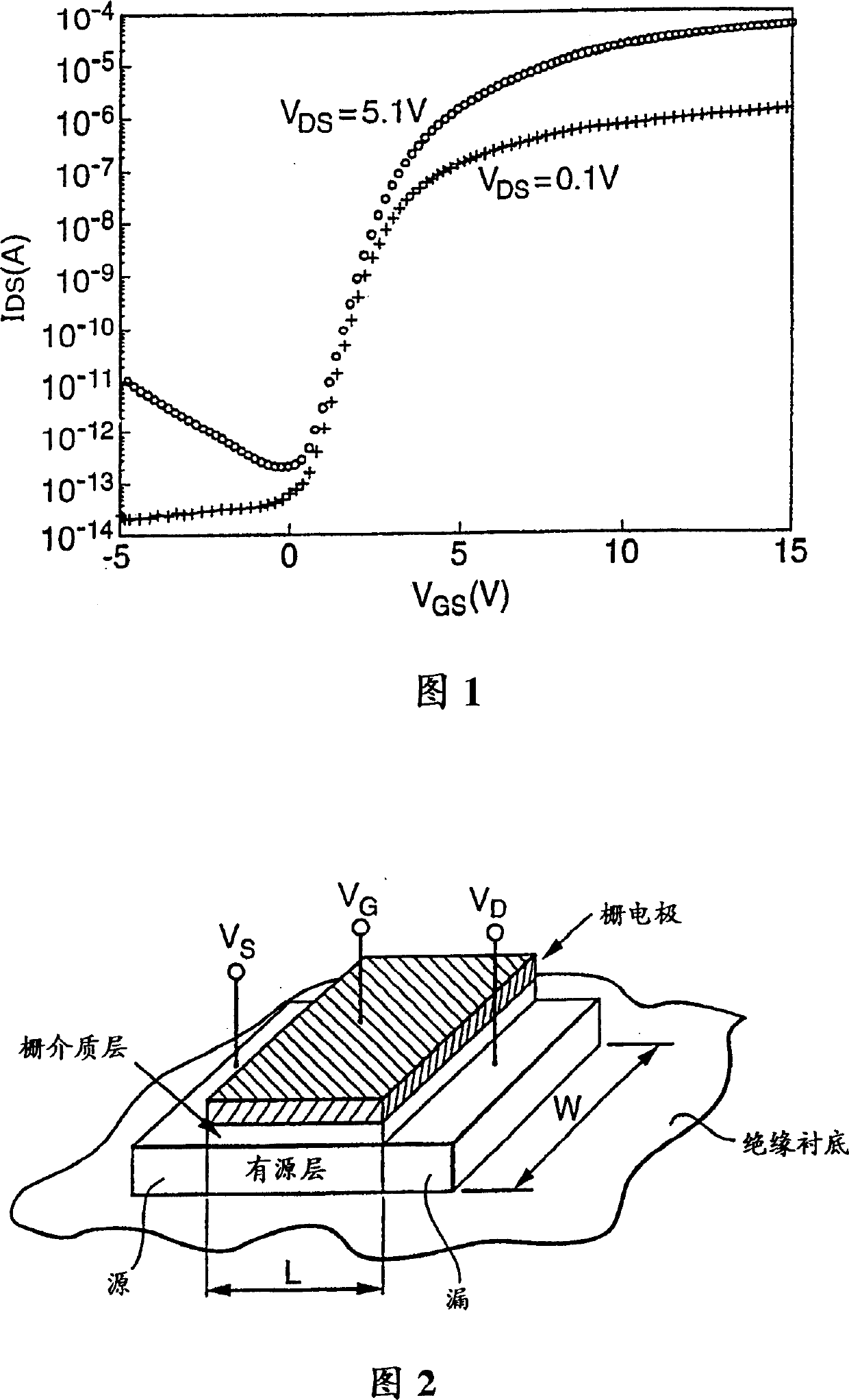
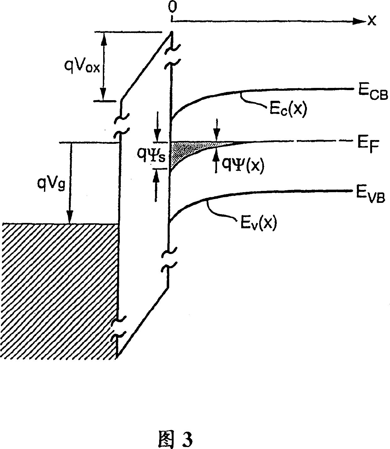
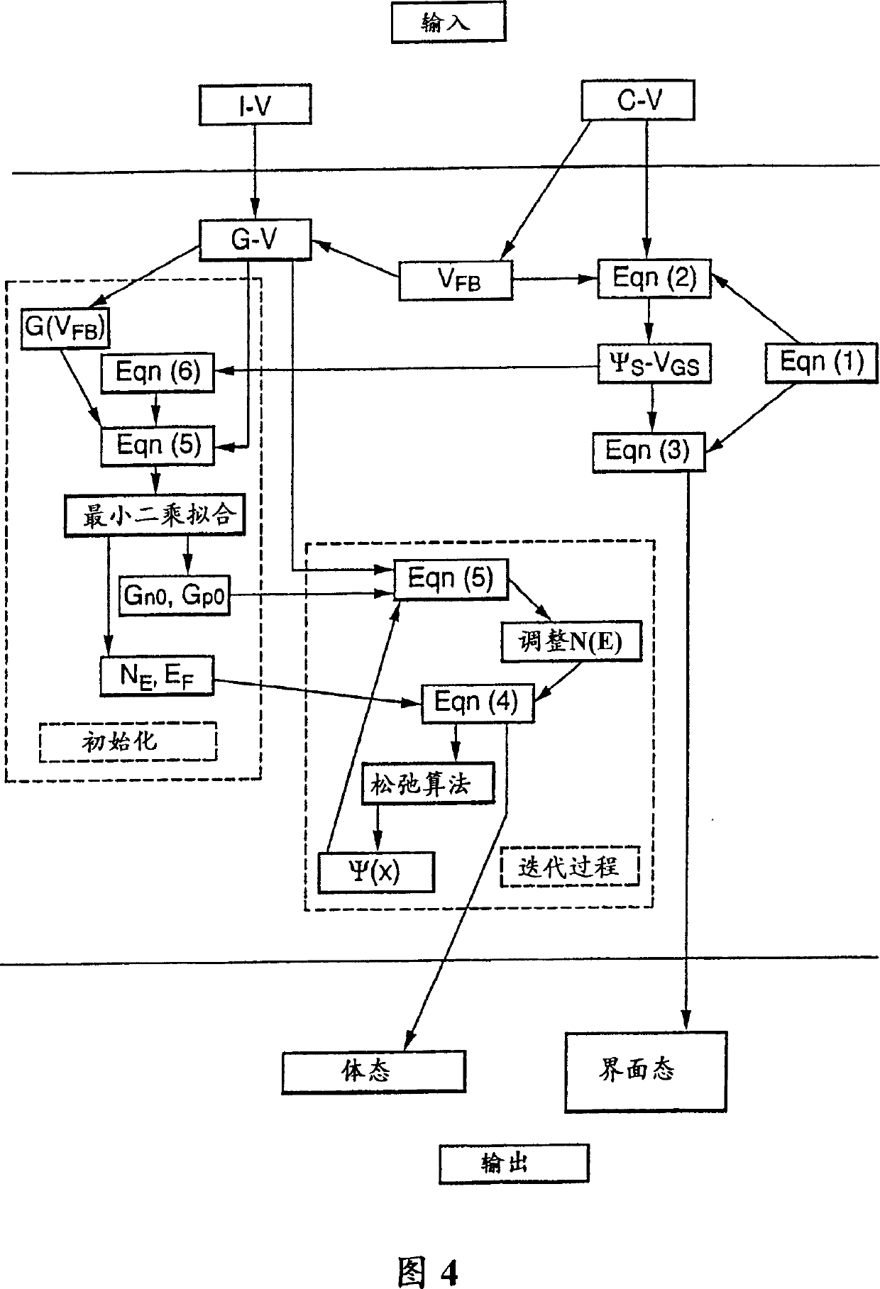
[0046] Fig. 2 illustrates the structure of a typical polysilicon TFT, indicating the structure dimensions referred to hereafter. FIG. 3 is an energy band diagram of the TF...


PUM


Abstract

A device and automated method of calculating bulk states information and interface states information of a thin film transistor from a current-voltage measurement and a capacitance-voltage measurement comprising the steps of: calculating the flat band voltage from the input capacitance-voltage measurement; applying a general expression of Gauss's Law and the calculated flat band voltage to a capacitance voltage relationship which defines capacitance so as to calculate a relationship between gate surface potential and gate/source voltage; applying Gauss's Law to the calculated relationship between gate surface potential and gate/source voltage to thereby calculate and ouput the interface states; calculating conductance/gate voltage data from the current-voltage measurement using the calculated flat band voltage; conducting an initialisation process using the calculated conductance/gate voltage data and the calculated relationship between gate surface potential and gate/source voltage, said initialisation process using a conductance equation so as to calculate initialised values for the electron conductance at the flat band voltage, for the hole conductance at the flat band voltage, for a density of states function and for the Fermi Energy; conducting an iteration process based on Poisson's equation using the said initialised values calculated by the initialisation process and the calculated conductance/gate voltage data to thereby calculate and output the bulk states information.

Description

technical field [0001] The invention relates to a method and equipment for calculating the electrical properties of thin film transistor (TFT) materials. Background technique [0002] Considering the complexity and high cost of the fabrication process for producing thin film transistors, it is highly desirable, though not absolutely necessary, to use mathematical simulations, also commonly referred to as models, for the design and performance calculations of such transistors. The key to the model is to accurately calculate the electrical properties of thin-film transistor materials. So heretofore, a lot of manpower has been expended to develop methods to calculate the performance of such transistors. Such methods are usually embodied in computer programs and sold as general commercial products by developers or their agents to designers and manufacturers of thin film transistors and other semiconductor products including such transistors. [0003] The known methods for calc...

Claims


Application Information

Patent Timeline
IPC IPC(8): H01L29/00G01R31/26G01R31/28G06F17/50H01L29/786
CPCG01R31/2603G06F17/5036G01R31/2621G01R31/2837G06F30/367G06G7/62
Inventor B·卢伊P·米格利奥拉托
Owner SEIKO EPSON CORP
Why Eureka
Try Eureka