Device and method for removing thin layers on support material

A substrate and equipment technology, applied in the field of surface layer ablation process of thin film solar cells, can solve the problems of component contamination, damage to the substrate surface, etc.

Inactive Publication Date: 2005-07-20
壳牌太阳能股份有限公司
View PDF3 Cites 2 Cited by
  • Summary
  • Abstract
  • Description
  • Claims
  • Application Information

AI Technical Summary

Problems solved by technology

In addition to damaging the substrate surface and forming microcracks as described, these methods have the further disadvantage of typically requiring the workpiece to be subsequently placed in an ultrasonic chemical cleaning of the pool

Method used


Image

  • Device and method for removing thin layers on support material
  • Device and method for removing thin layers on support material
  • Device and method for removing thin layers on support material

Examples


Embodiment Construction

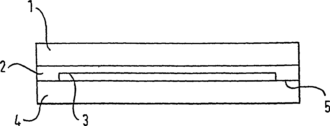
[0045] refer here figure 1 , illustrating a cross-section through an encapsulated thin-film solar cell. A solar cell actually comprises a substrate 4, a film layer 3 deposited and patterned thereon, a laminate layer 2 and a glazing layer applied thereon. The thickness of the carrier film layer 3 is in the range of 0.1 μm to 5 μm, and the substrate 4 is preferably made of float glass. In order to eliminate the current path to the current-carrying film layer 3 and to prevent moisture damage to the film itself, the surface region 5 of the substrate 4 does not contain a current-carrying layer. This is why the surface region 5 according to the invention is delaminated.

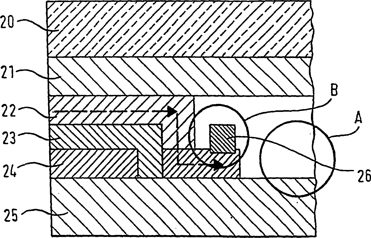
[0046] refer here figure 2 , illustrating a cross-section through an encapsulated thin-film solar cell showing the thin-film layer sequence and the contacting rear electrode. In substrate thin-film solar cells, the thin-film layer sequence consists of rear electrode 24 , absorber layer 23 and front electrode 2...


PUM

PropertyMeasurementUnit
wavelengthaaaaaaaaaa
thicknessaaaaaaaaaa

Abstract

The invention relates to a device and a method for removing thin layers on a support material, especially for removing barrier layers of a thin-layer solar cell. The aim of the invention is to provide an economical means of removing strips of up to a few millimetres in width without damaging the substrate of the thin-layer solar cell underlying the layer to be removed. To this end, a laser treatment device with a laser resonator and an optical system is provided. The optical system projects the treatment beam produced by the layer resonator over an area of 1 mm<2> to 1 cm<2> on the surface to be treated with an essentially homogenous distribution of power. Thin layers can be effectively removed from the substrate at pulse width of less than 100 ns and with a pulse energy density of 0.1 J / cm<2> to 10 J / cm<2>.

Description

technical field [0001] The present invention relates to a substrate film ablation method and apparatus thereof, for example, when delaminating laminated ceramics or laminated glass. More specifically, the present invention relates to surface layer ablation processes for thin film solar cells. Furthermore, the invention relates to a method for encapsulating a thin-film solar module comprising a thin-film laminate substrate. Background technique [0002] Traditional crystalline silicon solar modules are based on wafer fabrication and then electrical wiring, so as a rule relatively small power cells of about 1W silicon wafers are required to feed into 50-100W modules. [0003] Thin-film solar cells are known as variations of these conventional solar modules with micron thickness. The basic unit of a thin film solar cell is shown in figure 2 , which has a p / n junction between the absorber layer and the window layer. [0004] Unlike conventional wiring on silicon wafers, thin...

Claims


Application Information

Patent Timeline
Patent Type & Authority Patents(China)
IPC IPC(8): B23K26/00B23K26/06B23K26/073B23K26/08B23K26/36B23K101/40H01L31/04H01L31/18
CPCH01L31/18B23K26/0853B23K26/365B23K26/361
Inventor 赫尔穆特·沃格特弗朗茨·卡格
Owner 壳牌太阳能股份有限公司
Why Eureka
Try Eureka