

Piezo ink-jet head and shaking layer shaping method
A technology of vibrating layer and forming method, which is applied in printing and other directions, can solve the problems of unfavorable mass production, high difficulty, cumbersome process, etc., and achieve the effects of increased pass rate, reduced cost, and low process difficulty
- Summary
- Abstract
- Description
- Claims
- Application Information
AI Technical Summary
Problems solved by technology
Method used
Image

Examples
Embodiment 1
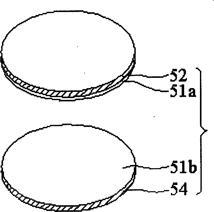
[0036] Such as Figures 3A to 3F , which shows a schematic cross-sectional view of the forming technology of the vibration layer of the piezoelectric inkjet head according to Embodiment 1 of the present invention.
[0037] Such as Figure 3A As shown, a first silicon chip 52 and a second silicon chip 54 are provided, and an oxidation process is performed to form a first SiO on the bonding surface of the first silicon chip 52. 2 layer 51a, and form a second SiO on the bonding surface of the second silicon chip 54 2 Layer 51b.
[0038] Such as Figure 3B As shown, silicon-on-insulator (SOI) technology is used to form a tight bond between the bottom of the first silicon chip 52 and the bonding surface of the second silicon chip 54 . In a preferred embodiment, a hydrogen-bonding solvent (such as acetone or alcohol) can be formed on the bottom surface of the first silicon chip 52 and the top surface of the second silicon chip 54 by spin coating or spraying. , so that the first...
Embodiment 2
[0046] The vibration layer forming technology of the piezoelectric inkjet head in the second embodiment of the present invention is roughly the same as the steps described in the first embodiment. Silicon technology, which can further reduce production costs and simplify the production process.
[0047] Such as Figures 4A to 4F , which shows a schematic cross-sectional view of the forming technology of the vibration layer of the piezoelectric inkjet head according to the second embodiment of the present invention.
[0048] Such as Figure 4A As shown, a first silicon chip 52 and a second silicon chip 54 are provided, and a first bonding layer 51c is formed on the bottom surface of the first silicon chip 52, and a second bonding layer 51c is formed on the top surface of the second silicon chip 54. Layer 51d. In a preferred embodiment, the bonding material of the first bonding layer 51c and the second bonding layer 51d can be: resin, phosphosilicate glass (PSG), spin on glas...
PUM
 Abstract
Description
Claims
Application Information