
High density semiconductor memory having diagonal bit lines and dual word lines

A memory and semiconductor technology, applied in semiconductor devices, digital memory information, semiconductor/solid-state device manufacturing, etc., can solve the problem of wasting chip area and so on

Inactive Publication Date: 2006-03-08
SIEMENS AG +1
View PDF0 Cites 0 Cited by
  • Summary
  • Abstract
  • Description
  • Claims
  • Application Information

AI Technical Summary

Problems solved by technology

[0011] exist Figure 1A In the structure of , the staggered pattern of bit lines connected to the local word line driver units between multiple memory blocks results in wasted chip area at the region Ap at the edge of each memory block

Method used


Image

  • High density semiconductor memory having diagonal bit lines and dual word lines
  • High density semiconductor memory having diagonal bit lines and dual word lines
  • High density semiconductor memory having diagonal bit lines and dual word lines

Examples


Embodiment Construction

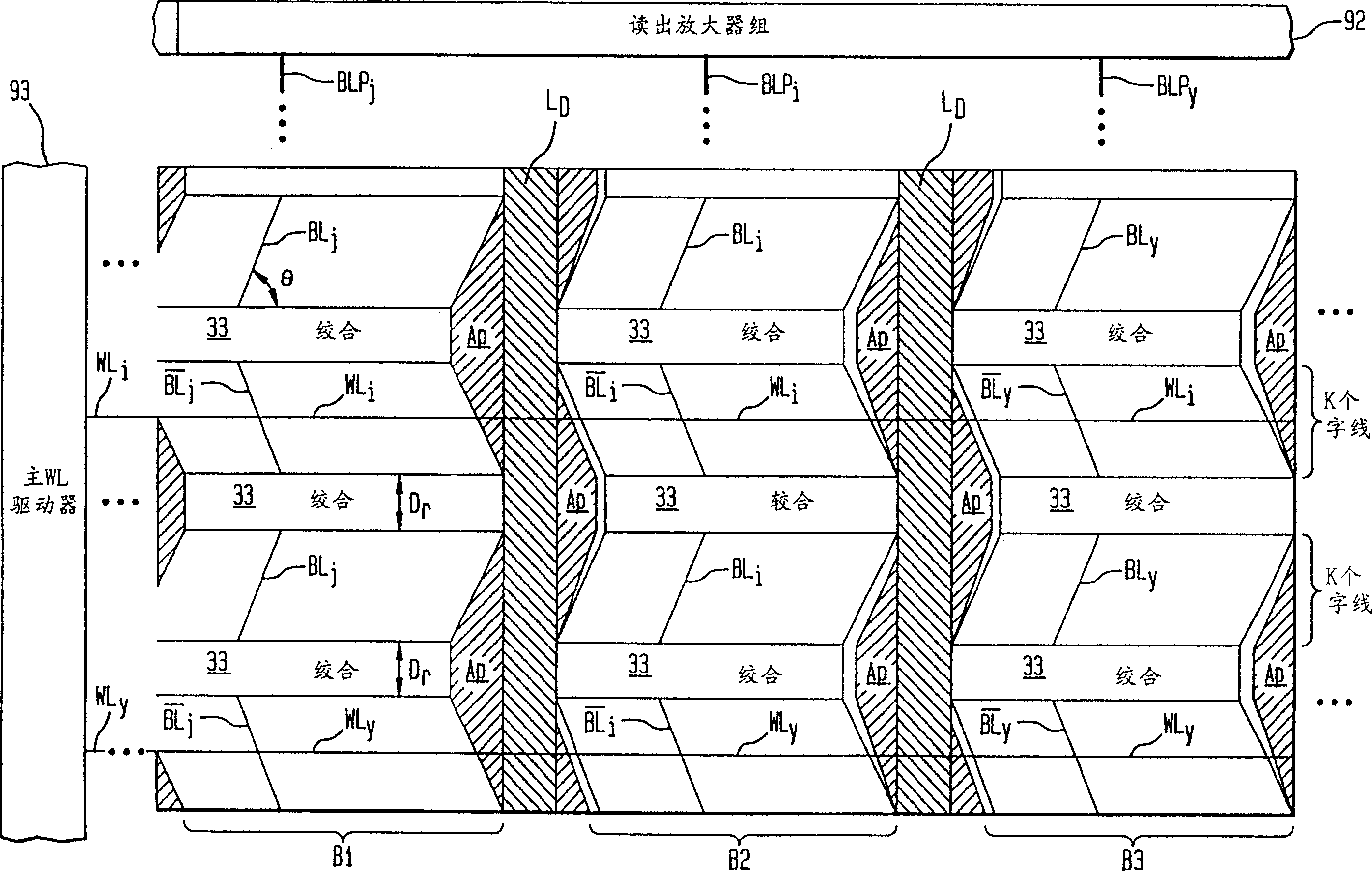
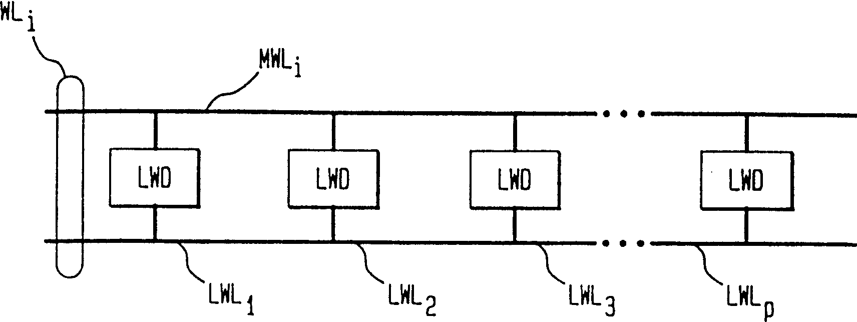
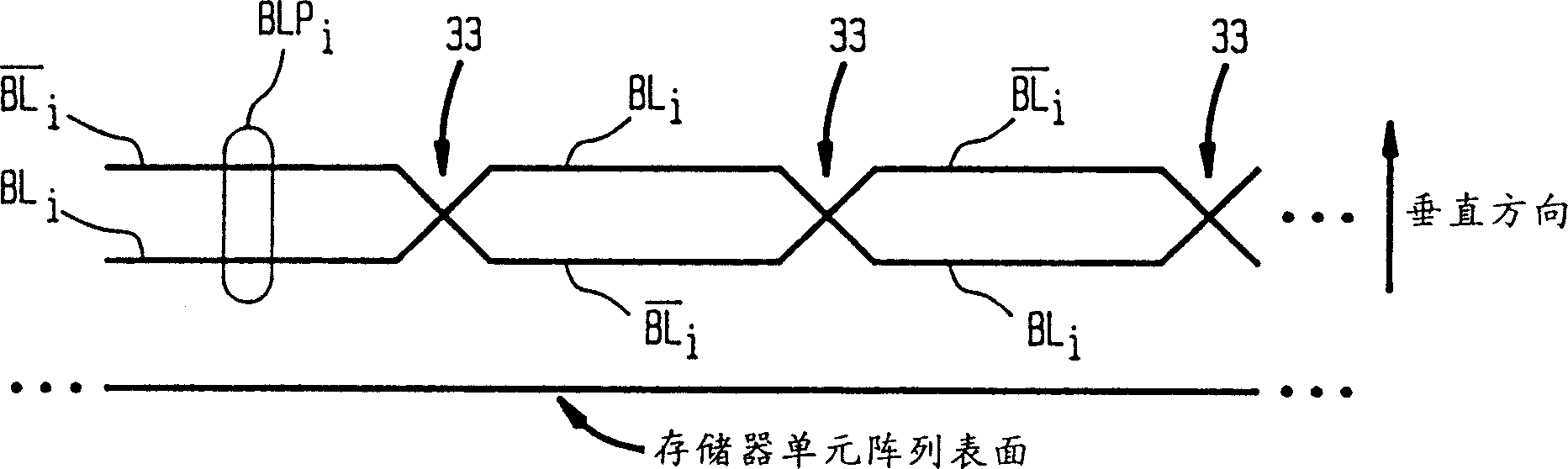
[0025] The present invention relates to a space efficient high density semiconductor memory using diagonal bit lines and double word lines having a space efficient structure. The present invention provides a method to substantially eliminate the area penalty associated with diagonal bitline memory. For purposes of discussion, exemplary embodiments of the present invention are described herein in the context of a DRAM chip. However, the invention has wider application. The invention is applicable to other memories such as EDO-DRAM, SDRAM, RAMBUS-DRAM, MDRAM, SRAM, Flash-RAM, EPROM, EEPROM or mask ROM or merged DRAM-logic (embedded DRAM), to name a few. Such devices may be used, for example, in consumer products such as computer systems, cellular telephones, personal digital assistants (PDAs), and other electronic products.

[0026] now for reference image 3, a simplified schematic block diagram of an embodiment of the present invention designated as DRAM 10 is shown here. ...


PUM


Abstract

Disclosed is a high density semiconductor memory having diagonal bit lines and a dual word line configuration. The present invention relates to The semiconductor memory includes a memory cell array of memory cells arranged in rows and columns, and a plurality of diagonal bit lines arranged in a pattern that changes horizontal direction along the memory cell array to facilitate access to said memory cells. The bit lines are arranged non-orthogonal to a plurality of dual word lines, where each dual word line includes a master word line at a first layer and a plurality of local word lines at a second layer. The local word lines are connected to the master word line of a common row via a plurality of spaced electrical connections, and each local word line is connected to plural memory cells. The electrical connections run in substantially the same pattern along the memory cell array as the bit lines.

Description

technical field [0001] The present invention generally relates to semiconductor memories such as dynamic random access memories (DRAMs). In particular, it relates to a space efficient structure for high density semiconductor memory having diagonal bit lines to facilitate access to memory cells, and double word lines on different vertically separated layers. Background technique [0002] Because there is a constant tendency to increase the capacity of semiconductor memories, new designs are required that save space on chips without compromising their performance. As smaller and smaller memory cells are realized, the problem of efficiently accessing the cells using wordlines and bitlines without additionally impacting the size of the chip becomes more and more challenging. [0003] Traditional DRAM chips use millions of memory cells arranged in rows and columns in one or more arrays, with bit lines parallel to the columns and word lines parallel to the rows. Each memory cell...

Claims


Application Information

Patent Timeline
Patent Type & Authority Patents(China)
IPC IPC(8): G11C11/40H10B12/00G11C7/18G11C11/4097
CPCH01L27/10891G11C7/18G11C11/4097H01L27/10861H10B12/038H10B12/488G11C8/14H10B12/482
Inventor 格哈德·米勒桐畑敏明海因茨·霍尼格施密德
Owner SIEMENS AG
Learn More