Wire frame, semiconductor device using such frame and its mfg. method
A manufacturing method and lead frame technology, applied in semiconductor/solid-state device manufacturing, semiconductor devices, semiconductor/solid-state device components, etc., can solve problems such as complex manufacturing process, high cost, and impossibility of miniaturization
- Summary
- Abstract
- Description
- Claims
- Application Information
AI Technical Summary
Problems solved by technology
Method used
Image

Examples
Embodiment 1
[0130] Next, Embodiment 1 of the present invention will be described with reference to the drawings.
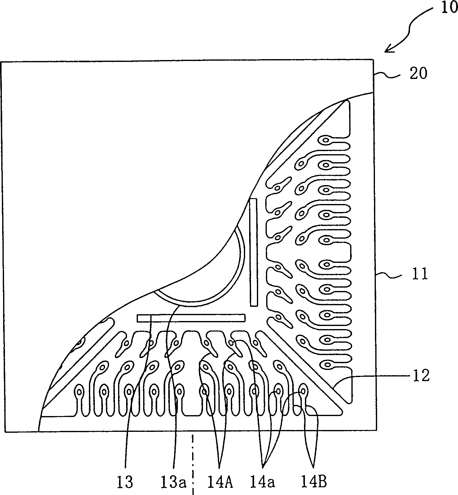
[0131] figure 1 It shows the bottom surface structure of the lead frame in Example 1 of the present invention, that is, the part including one die pad of the lead frame, and the lead frame is provided with a plurality of die pads of the inner inner lead portion before insulation processing.
[0132] Such as figure 1 As shown, the lead frame 10 has the following parts: a frame part 11; inside the frame part 11, the four corners are supported by the supporting wire part 12 as a connection support part, and on the top ( figure 1 The back side) holds the die pad portion 13 of the semiconductor element; is respectively supported by the peripheral portion of the die pad portion 13, and has a plurality of inner inner lead portions 14A having convex portions 14a on the bottom surface; disposed between the frame portion 11 and the inner inner lead portion 14A While extending inwa...
Embodiment 2
[0155] Embodiment 2 of the present invention will be described below with reference to the drawings.
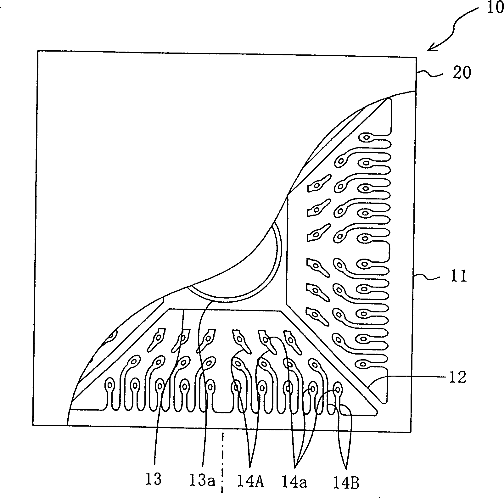
[0156] Figure 5 (a) and Figure 5 (b) is a resin-sealed semiconductor device according to Example 2 of the present invention, (a) is a plan view, and (b) shows an enlarged cross-sectional structure of (a) on line Vb-Vb. exist Figure 5 (a) and Figure 5 (b), for and figure 2 with image 3 The structural members that are the same as those shown are denoted by the same symbols, and their descriptions are omitted.
[0157] Figure 5 (a) and Figure 5 The resin-sealed semiconductor device 40 of the second embodiment shown in (b) uses the figure 2 The lead frame 10 of the shown embodiment 1 has the same structure as the lead frame, and the inner inner lead portion 14A and the outer inner lead portion 14B are both changed into two columns to form a four-row structure.
[0158] Such as Figure 5 As shown in (b), the resin-encapsulated semiconductor device 40 is composed...
Embodiment 3
[0173] Embodiment 3 of the present invention will be described below with reference to the drawings.
[0174] Image 6 (a) and Image 6 (b) is the lead frame of Example 3 of the present invention, and (a) shows the bottom surface structure including a part of one die pad of the lead frame on which a plurality of bosses before insulation (isolation) processing are provided. Die pad; (b) shows the cross-sectional structure on line VIb-VIb of (a).
[0175] Such as Image 6 (a) and Image 6 As shown in (b), the lead frame 30 includes: a frame portion 31; disposed inside the frame portion 31, on which a die pad portion 33 holding a semiconductor element is held; In three rows, the surface (bottom surface) opposite to the component holding surface has a plurality of inner lead portions 34 as convex portions of bosses.
[0176] Among the plurality of inner wire portions 34 , a part is supported by a frame connection support portion 32A as a first connection support portion exten...
PUM
 Abstract
Description
Claims
Application Information
 - R&D
- Intellectual Property
- Life Sciences
- Materials
- Tech Scout
- Unparalleled Data Quality
- Higher Quality Content
- 60% Fewer Hallucinations
Browse by: Latest US Patents, China's latest patents, Technical Efficacy Thesaurus, Application Domain, Technology Topic, Popular Technical Reports.
© 2025 PatSnap. All rights reserved.Legal|Privacy policy|Modern Slavery Act Transparency Statement|Sitemap|About US| Contact US: help@patsnap.com