Image display device using brilliance modulation device and its driving method

A technology of image display and luminance modulation, applied in lighting devices, electric solid state devices, semiconductor devices, etc.

Inactive Publication Date: 2006-07-26
HITACHI LTD
View PDF1 Cites 0 Cited by
  • Summary
  • Abstract
  • Description
  • Claims
  • Application Information

AI Technical Summary

Problems solved by technology

[0021] First, find the ineffective power consumption associated with the application of the scan pulse

Method used


Image

  • Image display device using brilliance modulation device and its driving method
  • Image display device using brilliance modulation device and its driving method
  • Image display device using brilliance modulation device and its driving method

Examples


Embodiment 1

[0142] The composition of the image display device of Embodiment 1 of the present invention is: by means of the combination of the thin-film electron source matrix and the phosphor which is the electron emission source itself, with the display panel having formed the luminance modulation device of each point, the drive Circuitry is connected to the row and column electrodes of the display panel.

[0143] The so-called thin-film electron source is an electron-emitting device with a structure in which an electron acceleration layer such as an insulating layer is inserted between two electrodes (upper electrode and lower electrode), and thermal electrons accelerated in the electron acceleration layer are passed through the upper part. A device in which electrodes emit into a vacuum. As examples of thin film electron sources, MIM electron sources made of metal-insulator-metal, ballistic electron surface emission devices using porous silicon etc. Japanese Journal of Applied Physic...

Embodiment 2

[0225] The display panel used in the image display device of the second embodiment of the present invention and the wiring method between the display panel and the driving circuit are the same as those of the first embodiment described above.

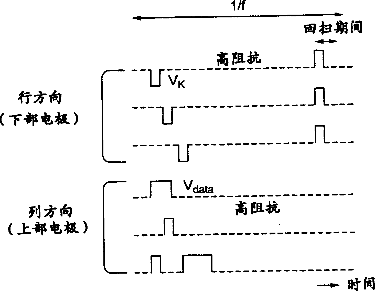
[0226] Figure 18 The timing chart of FIG. 10 shows an example of the waveforms of the driving voltages output from the row electrode driving circuit 41 and the column electrode driving circuit 42 in the image display device according to the second embodiment of the present invention.

[0227] During the period from time t1 to t2, V R1 After the scan pulse of , a scan pulse is applied to the row electrode 310R2 during time t2-t3 to control the electron emission from the thin film electron source on the row electrode 310R2. At this time, the adjacent row electrode 310R1 is connected to the ground potential not with high impedance but with low impedance. When a scan pulse is applied to the row electrode 310R3 during the period from time...

Embodiment 3

[0234] use Figure 22 The configuration of the display panel used in Embodiment 3 of the present invention will be described.

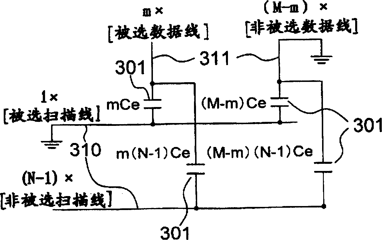
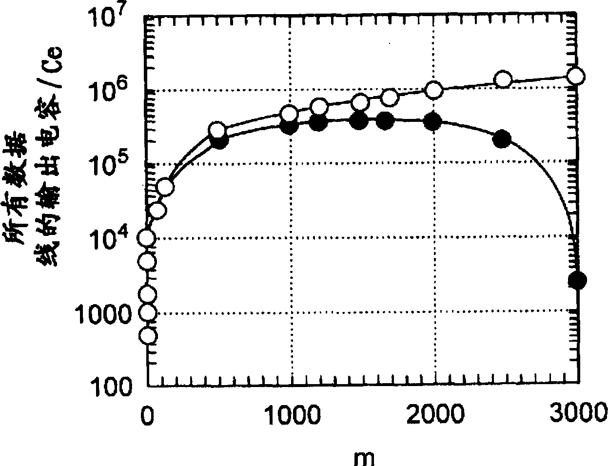
[0235] Although the display panel used in this embodiment is the same as that of Embodiment 1, as Figure 22 As shown, the point that the thin-film electron source device is formed as the dummy pixel 303 is different. The number of rows of thin-film electron source devices forming dummy pixels is defined as the ratio γ 0 There are more columns than M. Here ¶ 0 is γ that can be expressed by formula (9) 0 value. The dummy pixels 303 are formed between each row electrode 310 and a dummy column electrode 313 connected to the dummy column electrode driving circuit 45 .

[0236] But the fluorescent body 114 on the fluorescent display panel is only in contact with Figure 22 The area corresponding to the dotted line area is formed. That is, no phosphor is formed in the portion of the dummy pixel 303 . Therefore, since no light is emitted even if ele...


PUM


Abstract

A display apparatus includes a plurality of luminance modulation elements each modulated in luminance by a voltage of a positive polarity applied thereto, each of the luminance modulation elements being not modulated in luminance by a voltage of an opposite polarity applied thereto; a plurality of first lines electrically coupled to first electrodes of the plurality of luminance modulation elements; a plurality of second lines electrically coupled to second electrodes of the plurality of luminance modulation elements, the plurality of second lines intersecting the plurality of first lines; a first drive unit coupled to the plurality of first lines outputting scanning pulses; and a second driver unit coupled to the plurality of second lines. The first drive unit sets the first lines in a nonselection state to a high impedance state having a higher impedance as compared with the first lines in a selection state.

Description

technical field [0001] The present invention relates to an image display device and a driving method of the image display device, and particularly relates to a technique suitable and effective for an image display device in which a plurality of luminance modulation devices are arranged in a matrix. Background technique [0002] Among image display devices in which a plurality of luminance modulation devices are arranged in a matrix, there are liquid crystal displays, field emission displays (FED), organic electroluminescent displays, and the like. The so-called luminance modulation device is a device whose luminance changes depending on an applied voltage. Here, the luminance refers to transmittance or reflectance in the case of a liquid crystal display, and corresponds to the luminance of light emission in the case of a field emission display or an organic electroluminescent display. [0003] Such a display has an advantage that the thickness of the image display device ca...

Claims


Application Information

Patent Timeline
Patent Type & Authority Patents(China)
IPC IPC(8): G09G5/00G02F1/00H05B44/00G09G3/20G09G3/22G09G3/30G09G3/32H01J29/96H01L51/50
CPCG09G2310/065G09G3/22G09G3/20G09G2330/021G09G2320/0209G09G3/3216H01J29/96G09G3/2011G09G3/3266
Inventor 铃木睦三楠敏明佐川雅一
Owner HITACHI LTD
Why Eureka
Try Eureka