Field emission display made by single grid structure and silver pasting method

A grid structure and structure field technology, which is applied in the direction of image/graphic display tube, cathode ray tube/electron beam tube, cold cathode manufacturing, etc., can solve the complex manufacturing process of the grid structure, contamination or damage of the film surface, High electrical requirements and production requirements, to achieve the effect of complete packaging, avoid pollution and damage, and low cost

Inactive Publication Date: 2006-08-02
XI AN JIAOTONG UNIV
View PDF0 Cites 1 Cited by
  • Summary
  • Abstract
  • Description
  • Claims
  • Application Information

AI Technical Summary

Problems solved by technology

When fixing the cathode silicon chip, due to the large difference in thermal expansion coefficient between it and the packaging glass, there is a certain thermal stress, which is easy to cause the cathode glass panel to break during the high temperature sintering process, thus affecting the carbon of the three-pole field emission display. Assembly of nanotube membranes
[0003] In the device manufacturing process of the triode structure field emission display, the gate structure needs to be fabricated above the carbon nanotube film. The carbon nanotube film is very fragile, and it is very easy to pollute the surface of the film layer during the fabrication process of the gate structure. In addition, due to the high electrical requirements and production requirements of the gate base material, the fabrication process of the gate structure is complicated and the production cost is relatively high

Method used


Image

  • Field emission display made by single grid structure and silver pasting method
  • Field emission display made by single grid structure and silver pasting method
  • Field emission display made by single grid structure and silver pasting method

Examples


Embodiment Construction

[0032] The present invention will be further described below in conjunction with the accompanying drawings and embodiments, but the present invention is not limited to this embodiment.

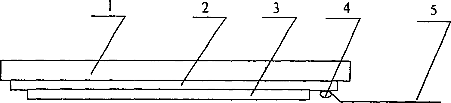
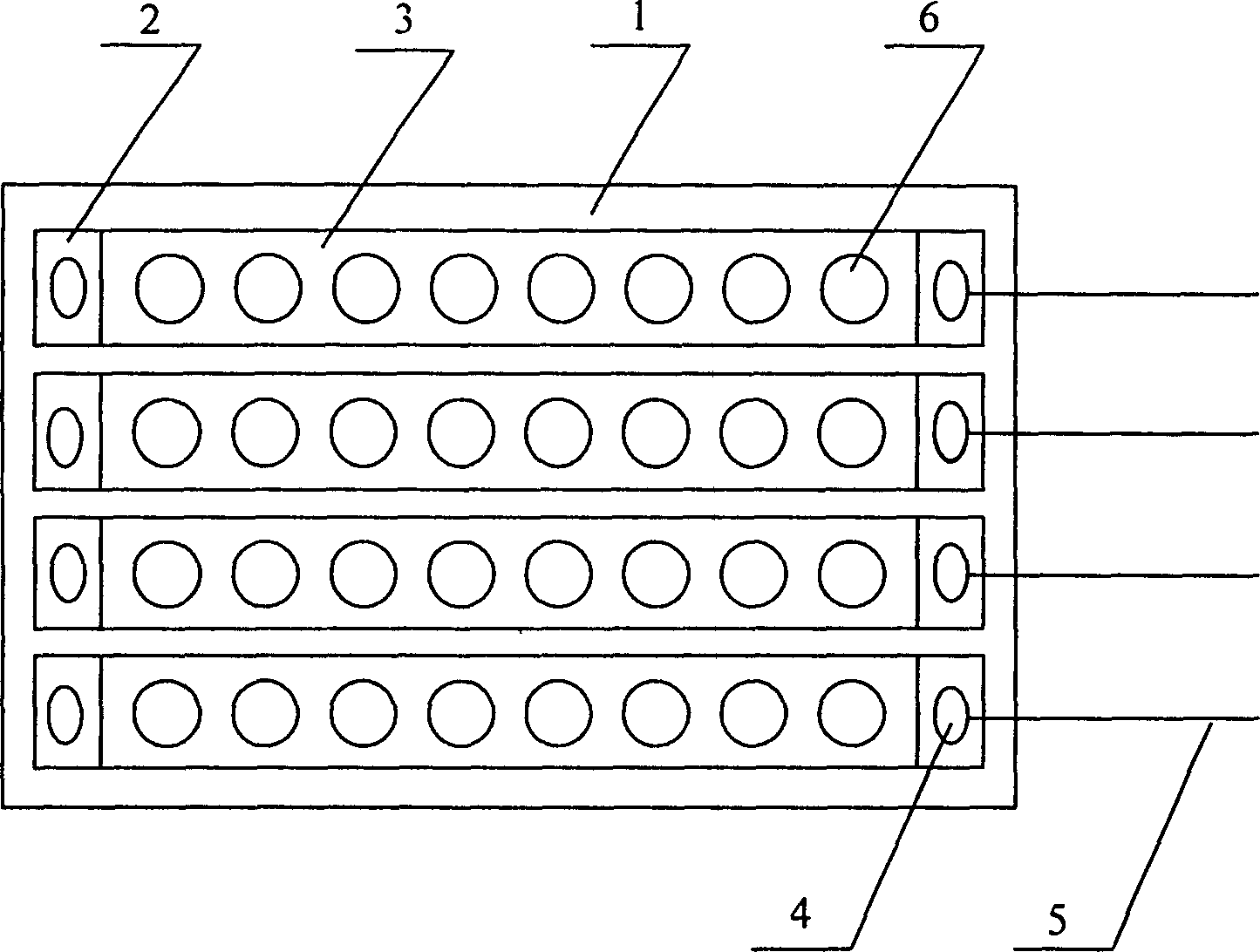
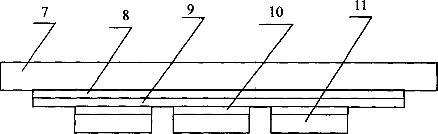
[0033] The three-pole field emission display of the present invention forms a sealed vacuum chamber by an anode panel 20, a cathode panel 12 and surrounding glass enclosures 13; photoetching forms an indium tin oxide transparent conductive film (Indium Tin Oxide, ITO) on the anode panel 12 18 conductive strips, printed on the ITO strip to form a phosphor layer 17; making isolation pillars 14 between the anode panel 12 and the control grid structure; using the substrate material 1 of the single grid, printed on the single grid substrate The silver paste layer on the material 1 and the insulating paste layer printed on the silver paste layer are used to form a single grid structure; the cathode lead wire arranged on the cathode panel and the cathode plate silver paste paste and fixation technolog...


PUM


Abstract

The invention discloses a field emission display made by singly-made grid structure and silver paste method, including anode panel, cathode panel, sealed vacuum cavity composed of four glass plates, and there is a indium tin oxide transparent conductive film and a fluorescent layer on the anode panel; there are gas outlet holes arranged on these glass plates; and its characters: there are also isolating brace and singly-made grid structure arranged in the sealed vacuum cavity and there is a cathode layer stuck and fixed on the cathode panel by the silver paste. It is simple to prepare, and increases the insulating intensity between the grid and nano carbon cathode; it adopts the technique of sticking and fixing cathode panel by silver paste, both implementing assembly and fixation of cathode silicon wafer and avoiding the smash of cathode glass panel (or silicon wafer) in the course of device sintering at high temperature, implementing the complete package of the whole device and simultaneously unnecessary to occupy the use space in the device and reducing the components for installing and fixing the cathode.

Description

technical field [0001] The invention belongs to the intersecting field of vacuum technology, microelectronic technology and nanotechnology, relates to a field emission flat panel display device, specifically relates to a screen printing A flat panel display device with the technology of pasting and fixing the conductive paste on the cathode plate, especially related to a kind of substrate material made by screen printing technology, using an independent thin-layer substrate as the substrate material of the control grid, using printed silver paste layer and insulating paste The manufacturing process of the control grid of the grid bar is made of layers, and the cathode panel structure is fabricated by the paste-fixing technology of the cathode plate conductive paste. Background technique [0002] At present, for a field emission display with a triode structure that uses a carbon nanotube film grown on a silicon wafer as an emitter, the carbon nan...

Claims


Application Information

Patent Timeline
Patent Type & Authority Patents(China)
IPC IPC(8): H01J29/02H01J31/12H01J9/02
Inventor 朱长纯李玉魁曾凡光刘兴辉刘卫华李昕
Owner XI AN JIAOTONG UNIV
Why Eureka
Try Eureka