Grinding process for back of wafer
A back-grinding and wafer technology, applied in electrical components, semiconductor/solid-state device manufacturing, circuits, etc., can solve the problems of wafer 20 fragmentation, collision damage, displacement deviation, etc., to reduce handling actions and prevent warpage and breakage. The effect of cracking and preventing chipping
- Summary
- Abstract
- Description
- Claims
- Application Information
AI Technical Summary
Problems solved by technology
Method used
Image

Examples
Embodiment Construction
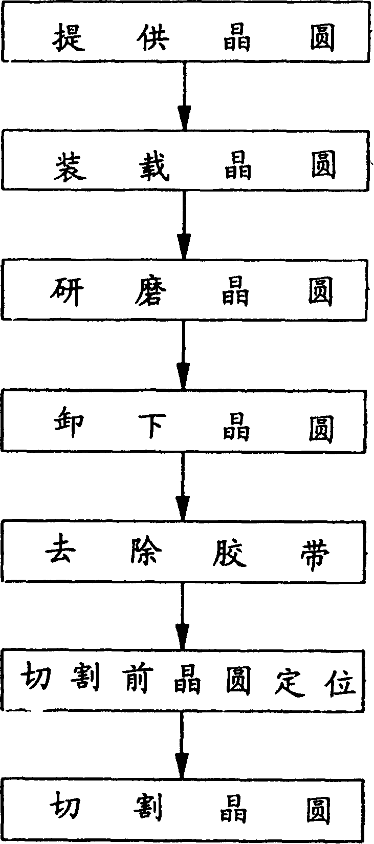
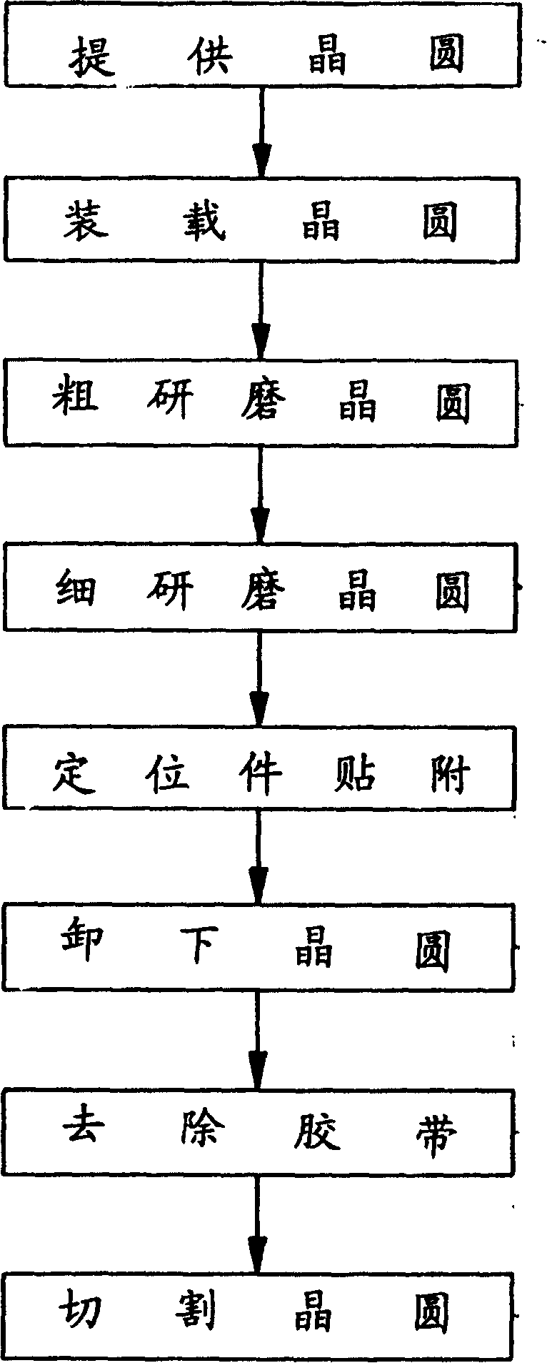
[0052] like image 3 , Figure 11 , Figure 12 Shown, the present invention comprises the steps:
[0053] step one
[0054] Provide wafer
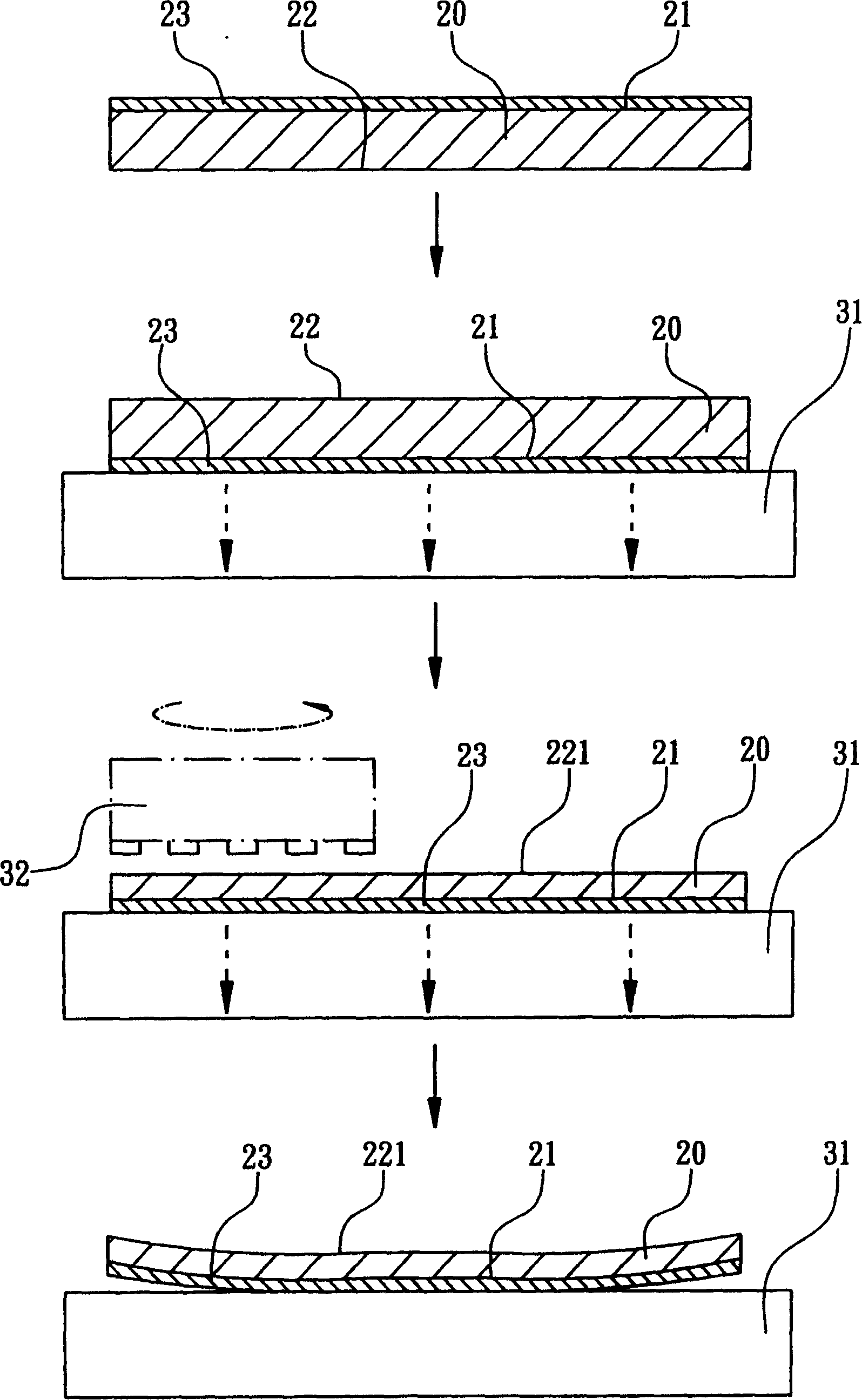
[0055] like Figure 4 As shown, a wafer 50 having an active surface 51 and a corresponding back surface 52 is prepared, and integrated circuits have been fabricated on the active surface 51, such as microprocessors, microcontrollers, memories or integrated circuits for special applications. Preferably, the wafer 50 is a high frequency memory, such as random access memory such as DDR, Rambus, TDR or QDR. The size of the wafer can be 4in, 5in, 6in, 8in or 12in, preferably, the wafer is 8in or 12in; preferably, a peelable adhesive protective tape 53 is attached to the active surface 51 of the wafer 50 .
[0056] step two
[0057] Load wafer
[0058] like Figure 5 As shown, the wafer 50 is loaded on the grinding chuck 61 of the wafer back grinding equipment 90 by vacuum adsorption or electrostatic adsorption, and the back surface 52...
PUM
 Abstract
Description
Claims
Application Information
 - R&D
- Intellectual Property
- Life Sciences
- Materials
- Tech Scout
- Unparalleled Data Quality
- Higher Quality Content
- 60% Fewer Hallucinations
Browse by: Latest US Patents, China's latest patents, Technical Efficacy Thesaurus, Application Domain, Technology Topic, Popular Technical Reports.
© 2025 PatSnap. All rights reserved.Legal|Privacy policy|Modern Slavery Act Transparency Statement|Sitemap|About US| Contact US: help@patsnap.com