Surface-mount antenna and communication device with surface-mount antenna

A surface-mounted, antenna technology, used in devices that make antennas work in different bands at the same time, antenna supports/mounting devices, antennas, etc., can solve the problem of capacitive coupling enhancement, inability to achieve multiple resonance conditions, resonance mutual interference, etc. question

Inactive Publication Date: 2001-11-07
MURATA MFG CO LTD
View PDF0 Cites 5 Cited by
  • Summary
  • Abstract
  • Description
  • Claims
  • Application Information

AI Technical Summary

Problems solved by technology

As a result, the capacitance of the coupling between the two radiation electrodes increases, and the capacitive coupling therebetween is strengthened, causing the resonance generated between the two radiation electrodes to interfere with each other
This creates a problem that one of the two radiating electrodes hardly resonates, making it impossi

Method used


Image

  • Surface-mount antenna and communication device with surface-mount antenna
  • Surface-mount antenna and communication device with surface-mount antenna
  • Surface-mount antenna and communication device with surface-mount antenna

Examples


Embodiment 1

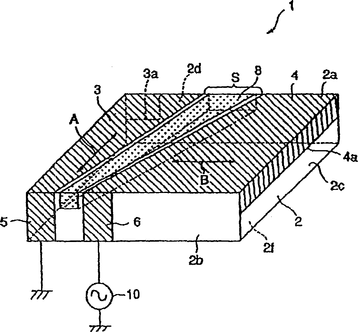
[0029] figure 1 is a schematic perspective view of a surface mount type antenna related to Embodiment 1 of the present invention. figure 1 The shown surface mount type antenna 1 has a dielectric base layer 2; on the top surface 2a of the dielectric base layer 2, a non-power supply terminal radiation electrode 3 as a first radiation electrode and a power supply terminal radiation electrode 4 as a second radiation electrode are formed. , with a space in between. In this Embodiment 1, the space S is formed between the non-power supply terminal radiation electrode 3 and the power supply terminal radiation electrode 4 such that its longitudinal sides are inclined (for example, at 45 degrees) with respect to each side of the top surface 2 a of the dielectric underlayer 2 . horn).

[0030] On one side surface 2b of the dielectric base layer 2, a ground electrode 5 connected to the non-power supply radiation electrode 3 and a power supply electrode 6 connected to the power supply ...

Embodiment 2

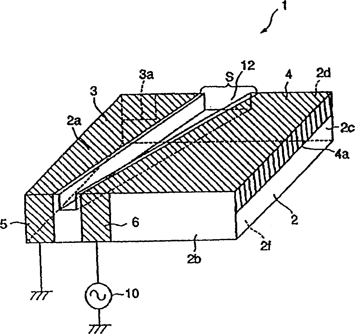
[0042] Such as figure 2 As shown, the difference between Embodiment 2 and the above Embodiment 1 in terms of features is that a groove 12 is provided as a capacitive coupling device instead of between the radiation electrode 3 at the non-power supply end and the radiation electrode 4 at the power supply end. A dielectric constant adjusting material portion 8 is provided. Other features are the same as those of Embodiment 1. In Embodiment 2, the same reference numerals are given to the same components as those of Embodiment 1, and repeated description of common components therebetween will be omitted.

[0043] As in the case of Embodiment 1, the surface mount antenna provided by Embodiment 2 is also arranged to weaken the capacitive coupling between the radiation electrode 3 at the non-power supply end and the radiation electrode 4 at the power supply end. In particular, the grooves 12, which are characteristic of Embodiment 2, are provided along the respective longitudinal ...

Embodiment 3

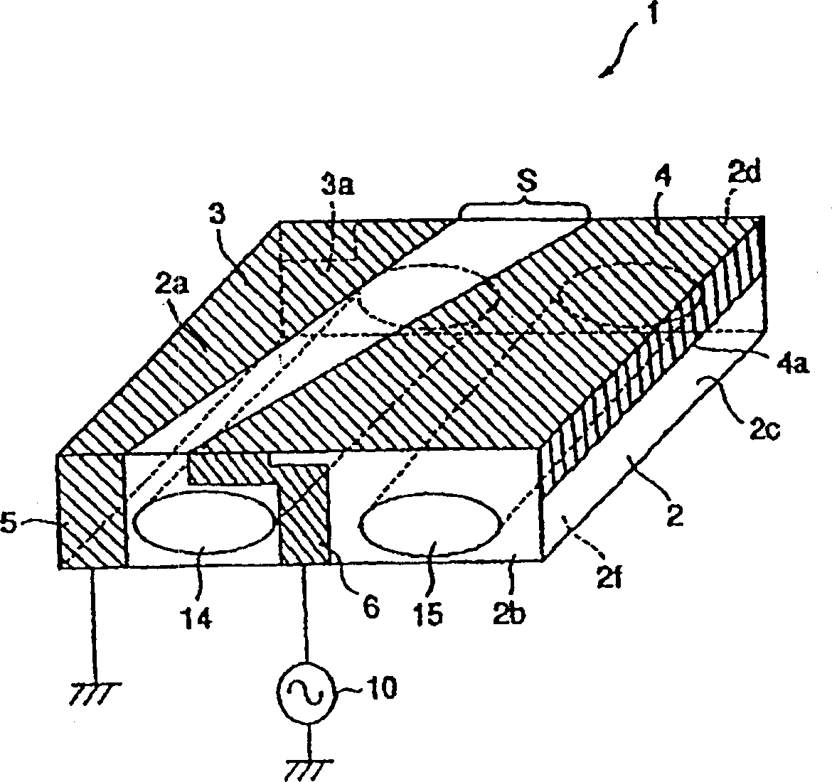
[0046] Such as image 3 As shown, Embodiment 3 is characterized in that there are hollow portions 14 and 15 in the dielectric bottom layer 2 as capacitive coupling adjusting means. Other features are the same as those of the above-mentioned embodiments. In this embodiment 3, the same reference numerals are given to the same parts as those of the above-mentioned embodiment, and repeated description of common parts therebetween will be omitted.

[0047] Such as image 3 As shown, in Embodiment 3, the hollow portion 14 is located in the region of the non-power-supply-side radiation electrode 3 in the dielectric bottom layer 2, and the hollow portion 15 is provided together with the hollow portion 14 at a distance therefrom.

[0048] According to the third embodiment, since the hollow portion 14 is formed in the region of the non-power supply side radiation electrode 3 within the dielectric substrate 2, the hollow portion 14 allows the capacitance between the non-power supply si...


PUM


Abstract

A parasitic radiation electrode (3) and a driven radiation electrode (4) are formed at an interval on the surface of a dielectric base (2). A material (8) for permittivity adjustment is provided in an interval (S) between the parasitic radiation electrode (3) and the driven radiation electrode (4) where capacitance is created. The material (8) for permittivity adjustment has a lower permittivity than the dielectric base (2), so that the permittivity between the parasitic radiation electrode (3) and the driven radiation electrode (4) is below the permittivity of the dielectric base (2), reducing the capacitive coupling between the parasitic radiation electrode (3) and the driven radiation electrode (4). As a result, the resonance interaction between the parasitic radiation electrode (3) and the driven radiation electrode (4) decreases, thus improving antenna performance, without taking measures, such as an increase in the interval (S) between the parasitic radiation electrode (3) and the driven radiation electrode (4) and a decrease in permittivity of the dielectric bases (2), which may obstruct the miniaturization of a surface-mount antenna (1).

Description

technical field [0001] The present invention relates to a surface mount type antenna mounted on a circuit board and the like incorporated into various communication devices, and also to a communication device including the antenna. Background technique [0002] In communication devices such as mobile phones, there are cases where a chip-shaped surface mount type antenna is mounted on a circuit board therein. There are many types of surface mount antennas. One of these is a multi-resonant surface mount antenna. [0003] This multi-resonance surface mount type antenna has a dielectric substrate made of a dielectric body (for example, ceramics or resin), and has two radiation electrodes on its surface with a space between the radiation electrodes. The resonant frequencies of the two radiating electrodes are set to deviate from each other so that if Figure 10 As shown by the frequencies f1 and f2 in , the transmission and reception frequency bands of the radio waves of the tw...

Claims


Application Information

Patent Timeline
IPC IPC(8): H01Q1/22H01Q1/24H01Q1/38H01Q1/52H01Q5/10H01Q9/04
CPCH01Q9/0407H01Q1/2283H01Q1/22H01Q1/243H01Q1/38H01Q1/521
Inventor 南云正二椿信人石原尚川端一也
Owner MURATA MFG CO LTD
Why Eureka
Try Eureka