Apparatus and method for an integrated circuit having high Q reactive components

A technology of integrated circuits and circuits, which is applied in the direction of printed electrical components, electrical components, circuits, etc., and can solve problems such as reducing the performance of functional circuits

Inactive Publication Date: 2002-02-27
ATMEL CORP
View PDF0 Cites 9 Cited by
  • Summary
  • Abstract
  • Description
  • Claims
  • Application Information

AI Technical Summary

Problems solved by technology

However, the parasitic reactance introduced by traditional packaging technology often seriously degrades the performance of functional circuits

Method used


Image

  • Apparatus and method for an integrated circuit having high Q reactive components
  • Apparatus and method for an integrated circuit having high Q reactive components
  • Apparatus and method for an integrated circuit having high Q reactive components

Examples


Embodiment Construction

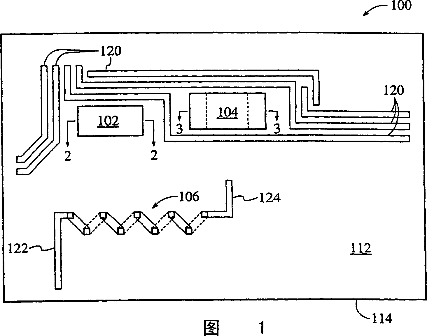
[0017] Figure 11 A typical ball grid IC package is shown, including a chip 1102 mounted on a substrate 1112 and encapsulated by an encapsulant 1110. Turning to Figure 1, a laminated substrate 114, configured in accordance with a preferred mode of the present invention, includes a single or multiple layers of interconnected metal layers, each layer being separated by a layer of insulating material. The uppermost interconnect layer shown in FIG. 1 includes a plurality of interconnect traces 120 and passive elements 102-106. Specifically, elements 102 and 104 are capacitors, while element 106 is an inductor. Inductor 106 can be seen to include traces 122 and 124 . This interconnect layer is disposed on the upper surface 112 of the substrate 114 .

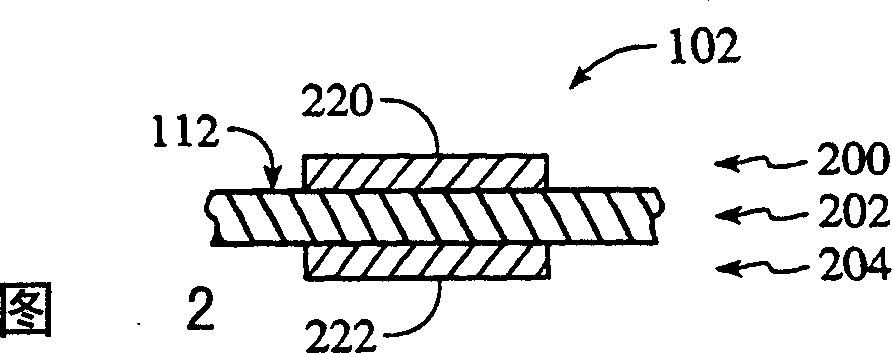
[0018] Referring to FIG. 2 , a side view of capacitor 102 taken along line 2 - 2 in FIG. 1 shows a portion of substrate 114 . A metal layer 200 is placed on top of insulating layer 202, which is also placed on another metal layer 2...


PUM


Abstract

In an IC packaging scheme, a multilayer substrate is composed of electrically conductive layers of interconnects, separated by insulative layers of epoxy resin or ceramic and connected by vias. Passive elements are integrated within the substrate at the definition stage during layout of the interconnects. The passives can be used to enhance the electrical performance of the active circuit die to a maximum extent allowed by the material technology used for the substrate. Material selection for the package is made to allow for the best passive integration for a given circuit design. Typical applications include power supply bypass capacitors, radio frequency tuning, and impedance matching. The incorporation of passives in the packaging substrate creates a new class of electrically tailorable packaging that can derive improved performance for any given die design over existing approaches.

Description

technical field [0001] The present invention generally relates to packaging of semiconductor devices, and is particularly directed to the fabrication of high-Q reactive components in such packages. Background technique [0002] The present invention relates to the structure of high-Q passive components, which are generally referred to, for example, as components used in radio frequency equipment. The difficulty with which these components are introduced in semiconductor chips is well known: the quality factor (Q) of the lumped and dispersed reactance parts is mainly dependent on the resistance of the metal, dielectric losses and parasitic reactances. The true value of the inductance and capacitance of lumped elements is greatly limited by the area available on the semiconductor chip. Similarly, distributed transmission line resonators are difficult to deploy at the desired frequency on a semiconductor chip due to space constraints. A common convention is to place the lumpe...

Claims


Application Information

Patent Timeline
Patent Type & Authority Applications(China)
IPC IPC(8): H01L23/12H01L23/538H01L23/66H01L25/00H01L25/16H01L27/06H01L27/08H05K1/16H05K3/46
CPCH01L23/5383H05K2201/097H01L2924/3011H05K2201/09263H01L2924/01079H05K3/4611H05K1/167H01L2224/16H01L23/5386H05K3/4644H05K1/162H05K1/165H01L2924/15311H01L23/66H05K2201/09672H01L27/08H05K2201/10674H01L27/0641H01L25/16H01L2224/16235H05K1/16
Inventor 小R·J·扎夫里尔D·C·鲍曼
Owner ATMEL CORP
Why Eureka
Try Eureka