Method and system of controlling taper growth in a semiconductor crystal growth process

A crystal growth and semiconductor technology, applied in the direction of crystal growth, single crystal growth, single crystal growth, etc., can solve the problem of not providing the repeatability of cone growth

Inactive Publication Date: 2002-05-22
MEMC ELECTONIC MATERIALS INC
View PDF7 Cites 17 Cited by
  • Summary
  • Abstract
  • Description
  • Claims
  • Application Information

AI Technical Summary

Problems solved by technology

Moreover, the control techniques taught in these patents do not provide adequate repeatability of cone growth.

Method used


Image

  • Method and system of controlling taper growth in a semiconductor crystal growth process
  • Method and system of controlling taper growth in a semiconductor crystal growth process
  • Method and system of controlling taper growth in a semiconductor crystal growth process

Examples


Embodiment Construction

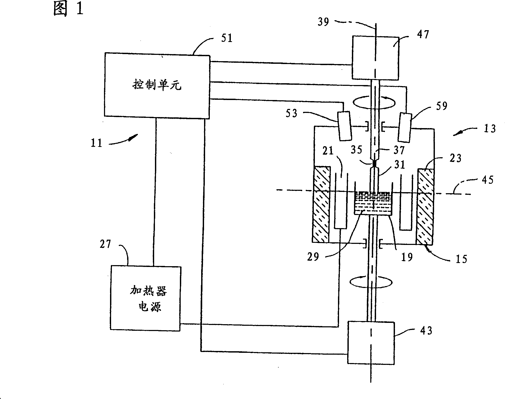
[0021] Referring now to system 11 shown in FIG. 1 for use with Czochralski crystal growth apparatus 13 . The detailed construction of crystal growth equipment is well known to those of ordinary skill in the art. In general, crystal growth apparatus 13 includes a vacuum chamber 15 containing a crucible 19 . A heating device such as a resistance heater 21 surrounds the crucible 19 . In one embodiment, insulating material 23 is lined at the inner walls of vacuum chamber 15 around which there is a water-permeable vacuum chamber cooling jacket (not shown). The vacuum pump typically evacuates the gas in the vacuum chamber 15 while argon gas, which is an inert gas, is introduced.

[0022] According to the Czochralski single crystal growth process, the crucible 19 is filled with a certain amount of polysilicon. The heater power supply 27 supplies current through the resistance heater 21 to melt the charged raw material, thereby forming a silicon melt 29 from which a single crystal ...


PUM


Abstract

A method and system for controlling growth of a taper portion of a semiconductor single crystal based on the slope of the taper. A crystal drive unit pulls the growing crystal from a melt at a target pull rate that substantially follows an initial velocity profile for growing the taper. A controller calculates a taper slope measurement as a function of a change in crystal diameter relative to a change in crystal length. The controller then generates an error signal as a function of the difference between the taper slope measurement and a target taper slope and provides a pull rate correction to the crystal drive unit as a function of the error signal. In turn, the crystal drive unit adjusts the pull rate according to the pull rate correction to reduce the difference between the taper slope measurement and the target taper slope. The target taper slope is defined by a function having a generally exponential component and a generally linear component.

Description

technical field [0001] The present invention relates generally to improved control of single crystal semiconductor growth processes for the manufacture of electronic components, and more particularly to a closed-loop method and system for precisely controlling the growth of cones in a Czochralski crystal growth process. Background technique [0002] Single crystal silicon is the raw material for most processes in the manufacture of semiconductor electronic components. Crystal pullers using the Czochralski process produce most of the monocrystalline silicon. Briefly, the Czochralski process involves the melting of high-purity polycrystalline silicon contained in specially designed quartz crucibles in a furnace. After heating the crucible to melt the contained silicon, the crystal lifting mechanism lowers the seed crystal to contact the molten silicon. The mechanism then pulls the growing crystal by pulling the seed crystal from the silicon melt. [0003] After the crystal ...

Claims


Application Information

Patent Timeline
Patent Type & Authority Applications(China)
IPC IPC(8): C30B15/20C30B15/22C30B29/06
CPCC30B15/20C30B15/22Y10T117/1004Y10T117/1008
Inventor 史蒂文·L·金贝尔罗伯特·R·万德三世
Owner MEMC ELECTONIC MATERIALS INC
Why Eureka
Try Eureka