High-responsivity photoelectronic detector based on the polarization effect of III family nitride heterojunction structure

A photodetector, heterostructure technology, applied in photometry, electric solid state devices, optical radiation measurement, etc., can solve the problems of incompatibility of integration technology, incompatibility of electrodes, difficult cleavage and cutting, etc., to reduce surface recombination , high responsivity, reduce the effect of direct compounding

Inactive Publication Date: 2002-09-25
NANJING UNIV
View PDF1 Cites 11 Cited by
  • Summary
  • Abstract
  • Description
  • Claims
  • Application Information

AI Technical Summary

Problems solved by technology

US Patent NS5847397 provides a nitride photoconductive photodetector with sapphire as the substrate material, but its detection sensitivity can still be improved
Moreover, the current problems of phot

Method used


Image

  • High-responsivity photoelectronic detector based on the polarization effect of III family nitride heterojunction structure
  • High-responsivity photoelectronic detector based on the polarization effect of III family nitride heterojunction structure
  • High-responsivity photoelectronic detector based on the polarization effect of III family nitride heterojunction structure

Examples


Embodiment Construction

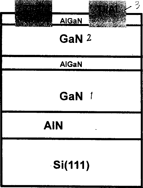
[0013] as the picture shows, figure 1 High-response photodetectors with medium-strain heterogeneous structures, grown on (111) (offcut about 3 degrees) high-resistivity silicon or sapphire (0001) substrate materials: Al x Ga 1-x N / GaN / Al y Ga 1-y N, x, y values ​​are 0.15-0.35, and on the top layer of Al y Ga 1-y Conductive electrodes are arranged on the N material. al x Ga 1-x N, GaN, Al y Ga 1-y The thicknesses of N are 15-30 nm, 50-80 nm, and 15-30 nm, respectively. Under the above conditions, a polarization electric field with a certain intensity directed to the substrate can be obtained.

[0014] Using silicon or sapphire as the substrate, aluminum nitride (AlN) as the buffer layer (thickness 100-300nm), gallium nitride (GaN) epitaxial layer (thickness 400-600nm) is grown on the buffer layer ie AlN in the figure ), and then grow Al on the epitaxial layer GaN 1 x G 1-x N / GaN / Al y Ga 1-y The N heterostructure serves as the light-absorbing region. The ranges ...


PUM

PropertyMeasurementUnit
Thicknessaaaaaaaaaa
Thicknessaaaaaaaaaa
Thicknessaaaaaaaaaa

Abstract

An optical detector has the following strain alloplasm materials on the silicon or sapphire gemstone substrate: with AIN as the buffer layer strain alloplasm structure GAN is grown extendedly. Polarized electric field arisen from the self-piezoelectric polarization effect especially for the strain alloplasm structure can effectively separate optical-electron-cavity couple to lower the direct complex lose to increase the lift of optical-carrier. Alloying metal electrode extends to the inner part of GAN from surface to reduce the surface complex loss of the carrier to raise the collective efficiency.

Description

technical field [0001] The invention relates to a semiconductor photodetector, in particular to a high-response photoconductive detector based on the polarization effect of a group III nitride heterostructure and a preparation method thereof. 2. Background technology [0002] Since the 1990s, the application research and development of semiconductor group III nitrides GaN, AlN, InN and their alloys AlGaN, InGaN and other wide bandgap materials and devices have been rapid. Photodetectors are one such device. The structure of existing detectors is mainly divided into two categories: photoconductive type and photovoltaic type (including p-n junction, Schottky junction, etc.), and the substrate materials of detectors include sapphire (sapphire), silicon (Si), etc. The material of the active region is GaN, AlGaN, InGaN, etc. to obtain responses in different wavelength ranges. The growth methods of materials mainly adopt metal organic compound vapor deposition (MOCVD) and molecu...

Claims


Application Information

Patent Timeline
IPC IPC(8): G01J1/02H01L27/14H01L31/00
Inventor 江若琏郑有炓沈波张荣顾书林胡立群施毅韩平朱顺明赵作明陈鹏
Owner NANJING UNIV
Why Eureka
Try Eureka