
High-efficient E type power amplifier optimized design method

A power amplifier and optimization design technology, applied in power amplifiers and other directions, can solve the problems of complicated design process, inability to guarantee performance meeting requirements, and energy consumption of matching network.

Inactive Publication Date: 2002-12-18
TSINGHUA UNIV
View PDF0 Cites 5 Cited by
  • Summary
  • Abstract
  • Description
  • Claims
  • Application Information

AI Technical Summary

Problems solved by technology

[0017] 1. Due to C 1 The selection of the value is somewhat arbitrary, and it cannot guarantee that the performance obtained in step (5) meets the requirements. Therefore, the actual design process often requires repeated attempts to make the PA meet the performance index requirements
The design process is more complicated
[0018] 2. Even if a solution that meets the performance requirements is obtained through repeated attempts, there is still no guarantee that this performance is the best among all the solutions
A mainstream direction of wireless technology development is low working voltage, but under the condition of given output power Pout, R L will become smaller, causing the matching network to consume more energy
The C selected by the above design method 1 is arbitrary, it is likely that R L values ​​become smaller, further exacerbating the problem

Method used


Image

  • High-efficient E type power amplifier optimized design method
  • High-efficient E type power amplifier optimized design method
  • High-efficient E type power amplifier optimized design method

Examples


Embodiment Construction

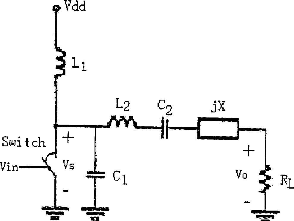
[0037] The embodiment of the high-efficiency Class E power amplifier optimal design method of the present invention is described as follows:

[0038] 1) Suppose the output power P out =150mW, power supply voltage V dd =1.5v, working frequency f=2.4GHz, output Q value

[0039] =10

[0040] 2) According to (Formula 6~8):

[0041] L 1 =9.91nH C 1 =2.22pF R L = 20.45 ohms

[0042] 3)L 2 =13.56nH, C 2 =0.324pF

[0043] 4) The theoretical calculation of X is relatively complicated. In the actual simulation process, another method can be used: gradually change the value of X until the waveform of each node meets the working conditions of class E PA, and then determine the value of X.


PUM


Abstract

This invention relates to high efficiency class E power amplifier optimizing design method including: a given system parameter: output power Pout, power voltage Vdd, working frequency f and output Q value OL(=2 pi F* / RL) and setting RL* the largest value (RL): to calculate elements C1, L1, and RL to get value C1*, L1* and RL*, then further calculate L2, C2, with numerical analysis method calculating reactance element value jx to simplify class E PA traditional design to get the largest optimizing load so as to reduce the matched network loss in creasing the entire efficiency of PA.

Description

technical field [0001] The technology belongs to the field of basic circuit design, and in particular relates to the circuit structure design of a power amplifier. Background technique [0002] The class E power amplifier (PA) circuit is composed of figure 1 As shown, it includes: a switch Sw connected to the input signal vin (usually a transistor is used, and the gate of the transistor is driven by the input signal vin to realize the switching function), an inductor L connected to the power supply voltage Vdd 1 and L 2 , capacitance C 1 One end is connected to the inductor L 1 and L 2 Between, the other end is grounded, the capacitor C 2 one end with L 2 Connected, the other end is connected to the reactance element jX, the load R L (In order to maximize the PA output power, R L Usually the best value is taken. Unless otherwise specified, R in the following L Both refer to the optimal load) one end is connected to the reactance element jX, the other end is grounde...

Claims


Application Information

Patent Timeline
IPC IPC(8): H03F3/20
Inventor 李永明胡海星
Owner TSINGHUA UNIV
Features
  • Generate Ideas
  • Intellectual Property
  • Life Sciences
  • Materials
  • Tech Scout
  • Unparalleled Data Quality
  • Higher Quality Content
  • 60% Fewer Hallucinations
Learn More