Method for controlling PWM pulse

A pulse control, vector technology, used in output power conversion devices, irreversible DC power input to AC power output, electrical components and other directions

Inactive Publication Date: 2003-03-26
YASKAWA DENKI KK
View PDF0 Cites 8 Cited by
  • Summary
  • Abstract
  • Description
  • Claims
  • Application Information

AI Technical Summary

Problems solved by technology

However, reducing the frequency of the PWM carrier signal creates a problem that the frequency of the current fluctuation component flowing into the motor is also reduced, thus increasing the frequency component that lies within the human hearing spectrum, which is generated by the current fluctuation component sound frequency components

Method used


Image

  • Method for controlling PWM pulse
  • Method for controlling PWM pulse
  • Method for controlling PWM pulse

Examples


no. 1 example

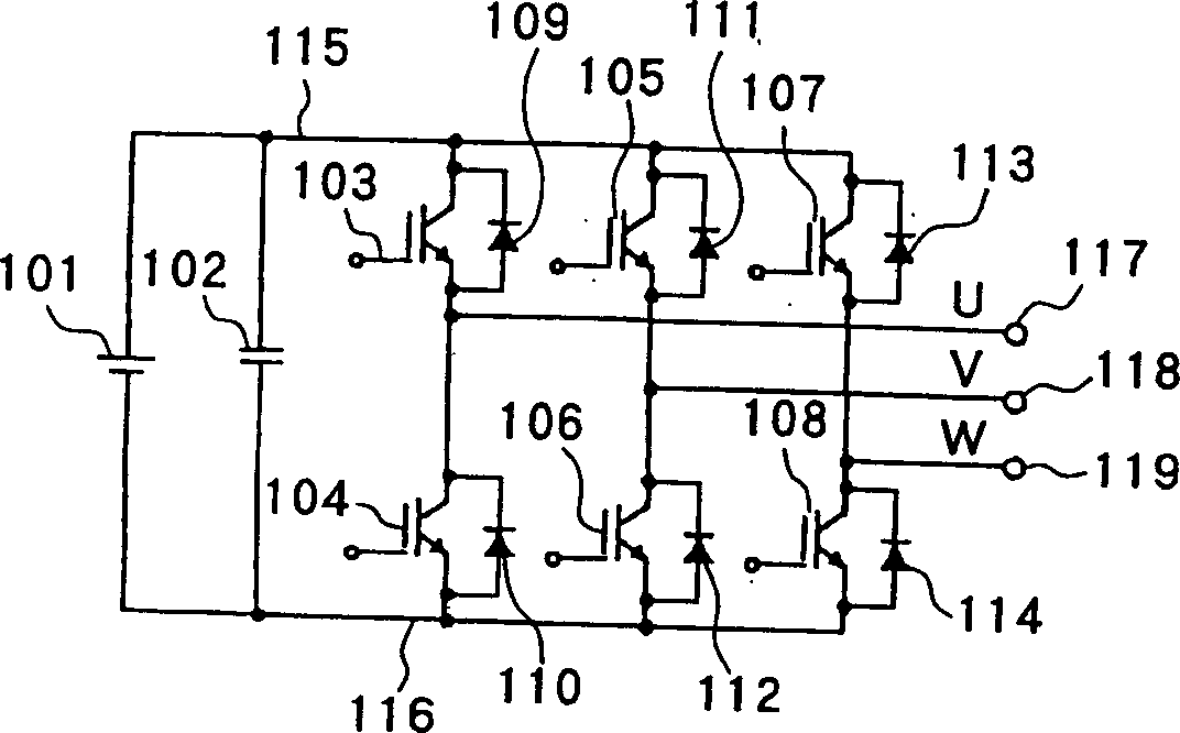
[0048] First refer to Figures 5 to 9 , to describe the PWM pulse control method of the first embodiment of the present invention in detail. The PWM pulse control method of this embodiment can be applied to such as figure 1 The three-phase two-bit PWM inverter shown. In this three-phase two-bit PWM inverter, three-phase modulation is used when the output frequency and modulation percentage are low.

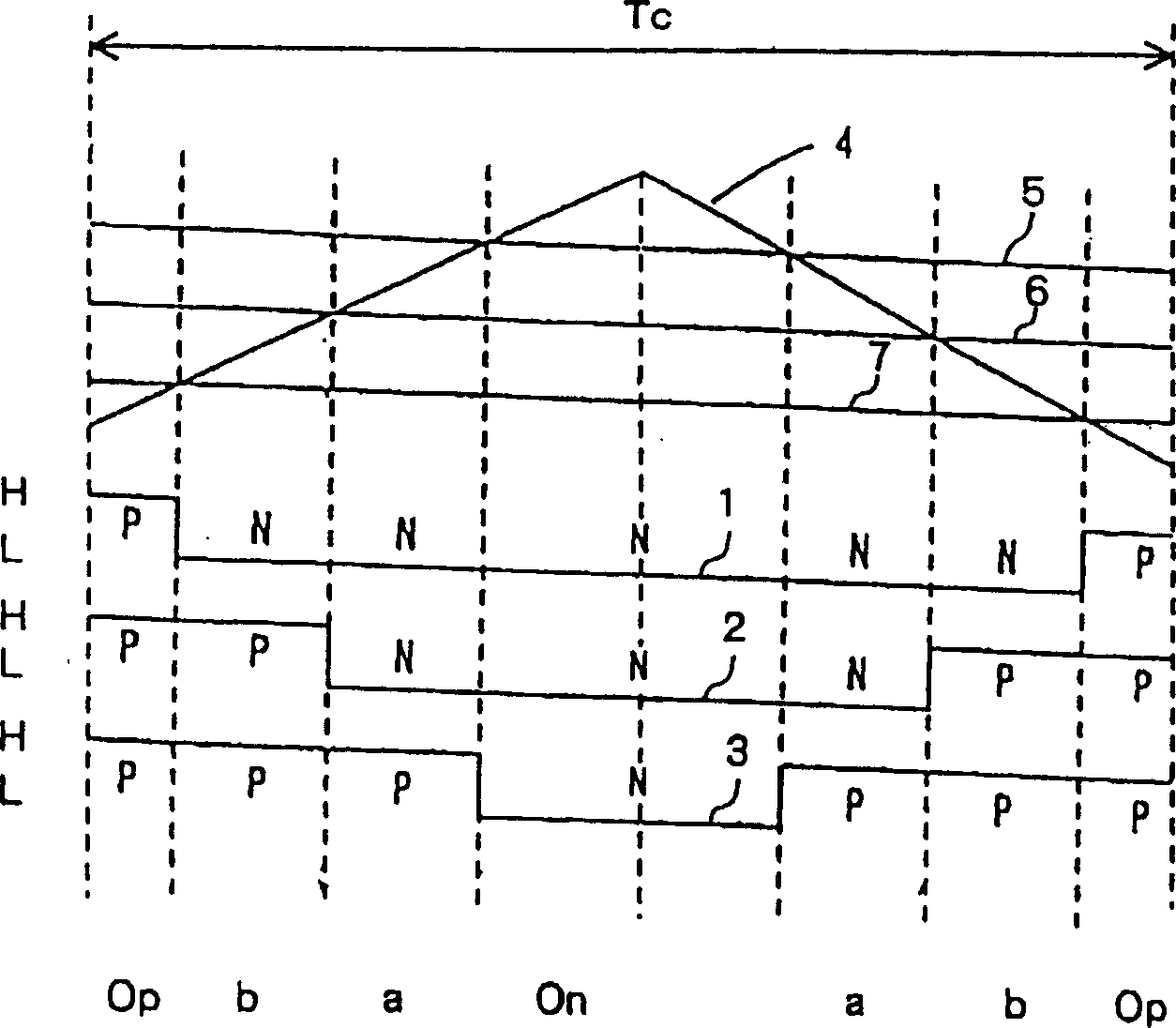
[0049] Figure 5 The timing chart shown represents the basic method in the PWM pulse control method described in this embodiment. Such as Figure 5 Shown in (a), in the PWM pulse control method of the present invention, just like the PWM pulse control method described in the prior art, when generating PWM pulse 1-3, observe the output sequence of each vector and output time. (Op-vector, b-vector) and (On-vector, a-vector) are divided into the next group, dividing the interior of one period Tc of the triangular waveform period 4 into time intervals, and in these time interval...

no. 2 example

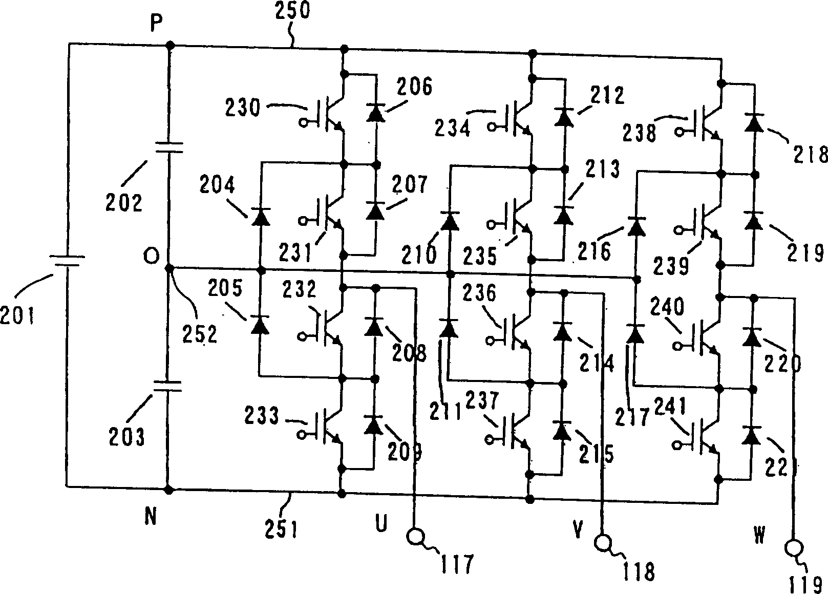
[0078] Refer below Figures 10 to 12 , to describe in detail the PWM pulse control method of the second embodiment of the present invention. The PWM pulse control method of this embodiment can be applied to image 3 The three-phase three-bit PWM inverter shown is the neutral point clamped inverter. With this three-phase three-bit PWM inverter, bipolar modulation is used when the output frequency and modulation percentage of the inverter are both low.

[0079] First refer to Figure 10, the timing diagram shown in this figure represents the basic method in the PWM pulse control method described in this embodiment. In the PWM pulse control method of the present embodiment, just like the PWM pulse control method described in the prior art, when generating PWM pulses 1-3, at first generate each vector in one period of the triangular waveform voltage 4 output sequence and output time.

[0080] In the prior art PWM pulse control method, the output time of each vector is as Fi...

no. 3 example

[0093] Refer below Figure 13 and 14 illustrate the PWM pulse control method according to the third embodiment of the present invention. Figure 7 and Figure 8 The control circuit and working process of the induction motor 305 using the PWM pulse control method described in the first embodiment are shown. However, in this control circuit, when the first set value m and the second set value n are the initial values ​​M1 and N1 respectively, the ON delay correction amount output from the ON delay correction amount operation unit 310 is ΔU", ΔV " and ΔW" are the ON delay correction amount.

[0094] As described above, the ON delay correction amount can be determined by generating the product of the ON delay time required to switch the semiconductor switching element once and the number of times of switching at a certain point of time, and since the number of times of switching is detected based on the number of divisions per vector, the When the initial values ​​M1 and N1 are...


PUM


Abstract

For the period where an Op vector and a b vector are outputted continuously among the periods where output voltage vectors of each phase are outputted in the PWM period, the output time of each vector is divided by a positive integer m to determine the division time of each vector, and the Op vector and b vector are outputted alternately and repeatedly m times for the division times. For the period where an On vector and an (a) vector are outputted continuously, the output time of each vector is divided by a positive integer n to determine the division time of each vector, and the On vector and (a) vector are outputted alternately and repeatedly n times for the divided times, thus spreading the frequency components of current ripple resulting from PWM pulses (1)-(3).

Description

technical field [0001] The present invention relates to a pulse width modulation (hereinafter abbreviated as "PWM") pulse control method used in power converters, such as inverters used in system interconnection or variable speed drives where the motor is the load, and more particularly , relates to a PWM pulse control method for enabling a three-phase driven inverter to perform low-noise operation. Background technique [0002] refer to figure 1 , the circuit diagram represents a three-phase two-level (two-level) PWM inverter structure. Such as figure 1 As shown, the three-phase two-position PWM inverter includes: DC power supply 101, capacitor 102, U-phase, V-phase and W-phase output terminals of a motor, semiconductor switching elements (such as IGBT and GTO) 103-108 and diodes 109-114. [0003] When the semiconductor switching elements 103, 105 and 107 are closed, the output terminals 117-119 for each phase are connected to the positive lead 115 drawn from the positi...

Claims


Application Information

Patent Timeline
Patent Type & Authority Applications(China)
IPC IPC(8): H02M7/48H02M7/483H02M7/5387
CPCH02M7/483H02M7/53873H02M2007/53876H02M7/53876H02M7/5387H02M7/48
Inventor 山中克利渡边英司寺田隆昭田中善之寺薗裕一
Owner YASKAWA DENKI KK
Why Eureka
Try Eureka