Eureka AIR delivers breakthrough ideas for toughest innovation challenges, trusted by R&D personnel around the world.

Antenna impedance matching method and device

A technology of antenna impedance and matching devices, which is applied to antennas, antenna parts, electrical components, etc., can solve the problems of impedance mismatch, difficult adjustment of the size and position of the converter, and difficult operation of the converter, so as to achieve easy impedance matching, Easy operation, simple principle effect

Inactive Publication Date: 2003-04-30
FOXCONN (KUNSHAN) COMPUTER CONNECTOR CO LTD +1
View PDF1 Cites 6 Cited by
  • Summary
  • Abstract
  • Description
  • Claims
  • Application Information

AI Technical Summary

Problems solved by technology

[0003] Impedance matching can be achieved by adding impedance converters such as 1 / 4 wavelength converters, branch matchers, etc. near the feed point. For related prior art, please refer to US Patent No. 6,239,765. The first conductor is located between the ground and the The part between the feed points is used as a 50Ω impedance converter, and its length is related to the operating frequency of the antenna. Through testing and adjustment, this impedance converter can simultaneously eliminate the input reactance of the antenna and make its input resistance equal to the characteristic impedance of the feeder line. But its disadvantage is that the size of the converter needs to be accurately calculated according to the operating frequency of the antenna. It is difficult to operate the converter when actually setting it up. Moreover, when the operating frequency of the antenna changes and the input impedance of the antenna changes, the size and position of the converter are not easy to adjust. Therefore, Impedance mismatch is often caused in practical applications

Method used


Image

  • Antenna impedance matching method and device
  • Antenna impedance matching method and device
  • Antenna impedance matching method and device

Examples


Embodiment Construction

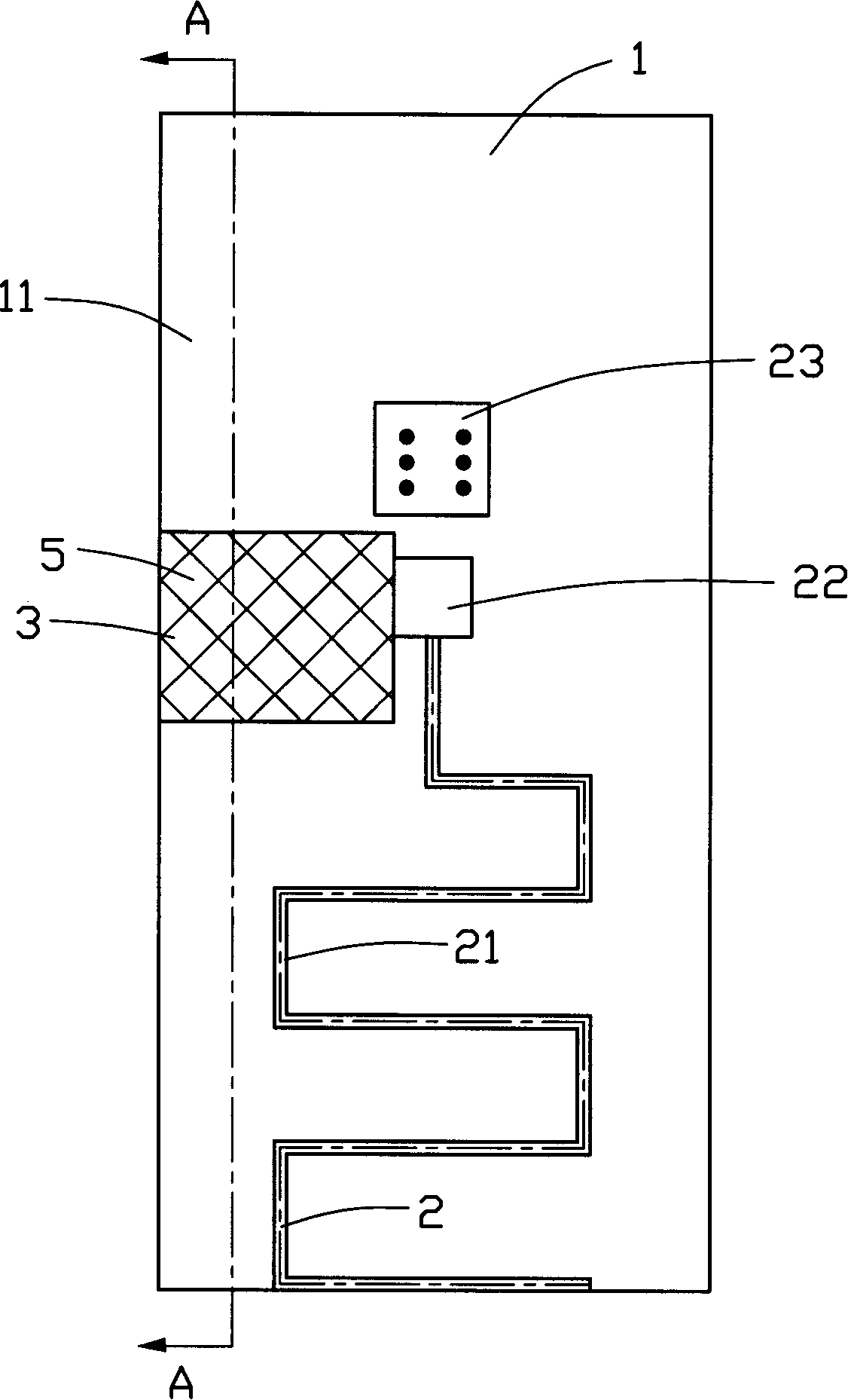
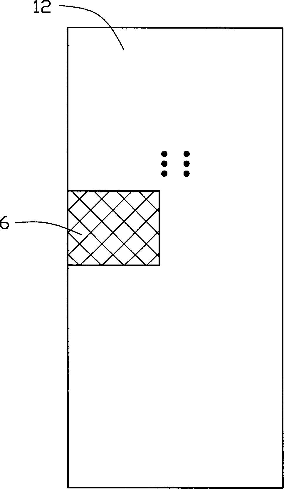
[0011] Please refer to figure 1 , figure 2 and image 3 , which represents a specific embodiment of the present invention, including a printed circuit board 1 , an antenna body 2 and an impedance matching device 3 . Wherein, the printed circuit board 1 includes an upper plane 11 and a lower plane 12 , the antenna body 2 includes a radiating portion 21 , a feeding portion 22 and a grounding portion 23 , and the impedance matching device 3 includes an upper metal sheet 5 and a lower metal sheet 6 .

[0012] The antenna body 2 and the upper metal sheet 5 are arranged on the upper plane 11, wherein the feeder 22 of the antenna body 2 is arranged at one end of the radiation portion 21 and is electrically connected with the radiation portion 21, and the grounding portion 23 is electrically connected to the feeder 22. If the antenna body 2 is fed by a coaxial cable (not shown), the inner core wire of the coaxial cable is electrically connected to the radiation part 21, and the gro...


PUM


Abstract

A impedance matching method for antenna sets upper and lower metal plates at the feed part antenna with printing circuit board to form a capacity and to utilize the pure reactance property of the capacity to eliminate the reactance part of antenna input impedance as well as the change the size of capatitance of capacity by adjusting the relative areas of upper and lower metal plates or by changing material of the printing circuit board for realizing the regulation of impetance matching so that the impedance matching can be easily achieved although the input reactance of antenna has been changed. The device for this method is the capacity formed by the conductive material and the media loaded in between. The capacity is connected with the feed part of antenna in electricity.

Description

【Technical field】 [0001] The invention relates to an antenna impedance matching method and its device, in particular to a printed circuit board antenna impedance matching method and its device. 【Background technique】 [0002] In the antenna system, it is necessary to transform the input impedance of the antenna to be equal to the characteristic impedance of the feeder line to ensure that there are only incident waves of signal voltage and current on the feeder line without reflected waves, that is, the antenna works in a traveling wave state, and the signal power is fully loaded by the antenna Absorption, this situation is an ideal situation, called impedance matching, at this time the voltage standing wave ratio is 1. The input impedance of the antenna is defined by the ratio of the voltage vector to the current vector at the feed point, including the input resistance and the input reactance. It also depends on the structure, size, operating frequency and the influence of t...

Claims


Application Information

Patent Timeline
Patent Type & Authority Applications(China)
IPC IPC(8): H01Q1/00
Inventor 黄建勋
Owner FOXCONN (KUNSHAN) COMPUTER CONNECTOR CO LTD
Why Eureka
Eureka Blog
Learn More