Groove component isolation structure
A component separation and groove type technology, which is applied in the manufacture of electrical components, semiconductor/solid-state devices, circuits, etc., can solve problems such as adverse effects on circuit work and difficulties in controlling the threshold voltage of transistors, and achieve the effects of improving manufacturing yield and preventing short circuits
- Summary
- Abstract
- Description
- Claims
- Application Information
AI Technical Summary
Problems solved by technology
Method used
Image

Examples
Embodiment 1
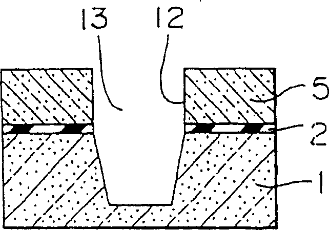
[0067] FIG. 1 shows a cross-sectional view of the manufacturing process of the trench-type component separation structure of Embodiment 1 of the present invention.
[0068] First, as shown in FIG. 1(a), on the substrate 1, a silicon oxide film of about 5 to 30 nm obtained by thermal oxidation, that is, the lower layer oxide film 2, and a polysilicon film 5 of about 100 to 300 nm are sequentially stacked. As the non-single crystal silicon film, the polysilicon film 5 and the lower layer oxide film 2 in the element isolation formation region are etched by anisotropic etching, and further, by etching the substrate 1 to a depth of about 100 to 500 nm, the substrate 1 is etched. A groove 13 is formed in the bottom.
[0069] Thus, groove 13 can be formed from the surface of polysilicon film 5 to silicon substrate 1 so that polysilicon film 5 has side wall portion 12 continuous with the side wall of the groove of silicon substrate 1 .
[0070] In addition, as the non-single crystal ...
Embodiment 2
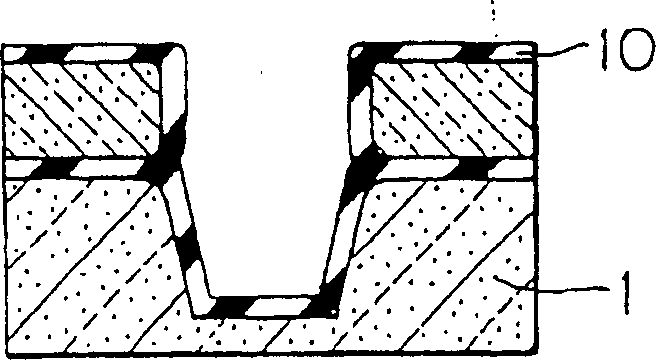
[0082] FIG. 2 shows a cross-sectional view of the manufacturing process of such a groove-shaped element separation structure according to Embodiment 2 of the present invention.
[0083] First, as shown in FIG. 2(a), on a substrate 1, a lower layer oxide film 2 composed of a silicon oxide film obtained by thermal oxidation with a film thickness of about 5 to 30 nm, and a film of about 30 to 100 nm are sequentially stacked. After the thick polysilicon film 5 and silicon nitride film 3 with a film thickness of about 100 to 300 nm, use anisotropic etching to open the silicon nitride film 3, polysilicon film 5, and lower oxide film 2 in the element isolation formation area, and then Grooves 13 are formed in the substrate by etching the substrate 1 to a depth of about 100 to 500 nm.
[0084] Next, as shown in FIG. 2(b), a thermally oxidized film 10 of about 5 to 50 mm is formed inside the trench by a thermal oxidation method. In such a process, the side wall portion 12 of the polys...
Embodiment 3
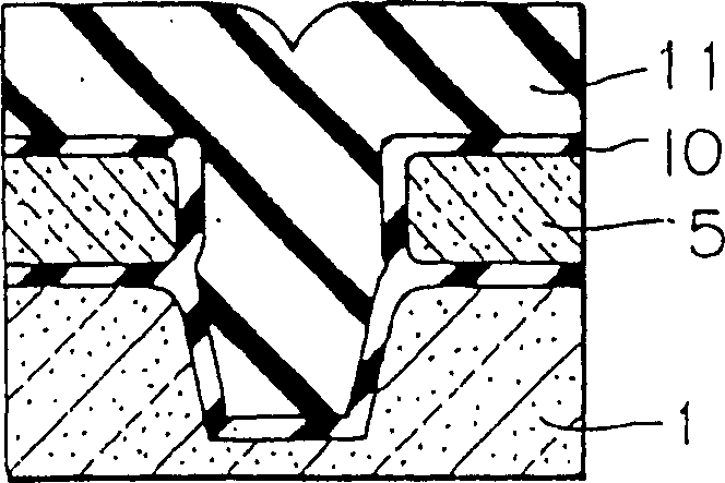
[0092] FIG. 3 shows a cross-sectional view of the manufacturing process of the trench-type element separation structure according to Embodiment 3 of the present invention.
[0093] When the width of the groove is narrowed along with the miniaturization of the device, the problem is that a seam as shown in FIG. 14 will occur. However, the third embodiment prevents such a seam. .
[0094] That is, when embedding the buried oxide film 11 by the conventional method shown in FIG. 13, if the aspect ratio of the groove becomes large, the embedding will be incomplete, and a seam 40 will occur inside the groove as shown in FIG. 14(a). . In FIG. 14, 1 denotes a substrate, 2 denotes a thermal oxide film, and 3 denotes a silicon nitride film.
[0095] As shown in Fig. 14 (b), (c), in the structure that has such seam 40, when removing silicon oxide film 2 with hydrofluoric acid, seam will be further enlarged, and in next step , the wiring material formed on the upper part of the groove ...
PUM
 Abstract
Description
Claims
Application Information
 - R&D
- Intellectual Property
- Life Sciences
- Materials
- Tech Scout
- Unparalleled Data Quality
- Higher Quality Content
- 60% Fewer Hallucinations
Browse by: Latest US Patents, China's latest patents, Technical Efficacy Thesaurus, Application Domain, Technology Topic, Popular Technical Reports.
© 2025 PatSnap. All rights reserved.Legal|Privacy policy|Modern Slavery Act Transparency Statement|Sitemap|About US| Contact US: help@patsnap.com