Surface acoustic wave device and method of manufacturing device

A surface acoustic wave device and surface acoustic wave technology, which is applied in the manufacture of electric solid devices, semiconductor devices, semiconductor/solid state devices, etc., can solve problems such as damage to output, failure to provide sealing characteristics, damage to cut off or separation, etc.

Inactive Publication Date: 2003-09-03
KK TOSHIBA
View PDF0 Cites 6 Cited by
  • Summary
  • Abstract
  • Description
  • Claims
  • Application Information

AI Technical Summary

Problems solved by technology

During this process, the SAW element may be damaged, chipped or separated between parts, failing to provide adequate sealing characteristics and destroying yield

Method used


Image

  • Surface acoustic wave device and method of manufacturing device
  • Surface acoustic wave device and method of manufacturing device
  • Surface acoustic wave device and method of manufacturing device

Examples


Embodiment 1

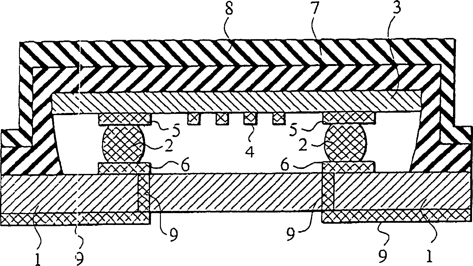
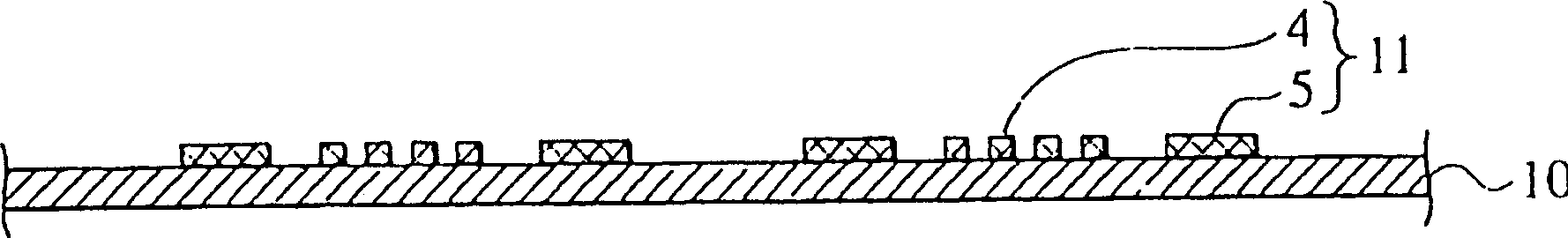
[0026] figure 1 is a sectional view showing a surface acoustic wave device according to Embodiment 1 of the present invention. The surface acoustic wave device according to Embodiment 1 has a base plate 1 with a predetermined line and electrode pads 6 formed on its front and rear faces; a striker 2 connected to the electrode pads 6 on the base plate 1; a surface acoustic wave element with Electrode sheet 5 and transducer 4 formed on the surface of piezoelectric substrate 3; and sealing materials 7 and 8, which are mechanically connected to chassis 1 and cover and seal the surface acoustic wave element.

[0027] On the back of the base plate 1, terminals 9 connected to the outside are formed, and a circuit pattern and electrode pads 6 connected to the terminals 9 are formed on the surface thereof. The striker 2 is a connection part that electrically and mechanically connects the electrode sheet 6 to the electrode sheet 5 . The surface acoustic wave element has a piezoelectric...

Embodiment 2

[0057] Figure 7 is a sectional view showing a surface acoustic wave device according to Embodiment 2 of the present invention. The surface acoustic wave device of embodiment 2 also has the base plate 1, the striker 2 and the surface acoustic wave element, and this instrument has the same arrangement as the base plate 1, the striker 2 and the surface acoustic wave element in the apparatus of embodiment 1. The sealing material is mechanically connected to the base plate 1, and together with the base plate covers and seals the surface acoustic wave element. The structure of the sealing material is different from that of Example 1, and it has a three-layer structure.

[0058]According to Embodiment 2, the sealing material is composed of the insulating resin 22 , the first sealing material 7 and the second sealing material 8 . The insulating resin 22 is, for example, polyvinyl alcohol resin. Application of the insulating resin 22 prevents a short circuit between the metal wirin...


PUM


Abstract

A surface acoustic wave device used in, for example, a mobile communications field as a filter or duplexer and the like to handle high frequencies of about several GHz is fabricated by flip-chip-connecting a surface of a piezoelectric substrate to a base board facing thereto, emitting particulate first sealing material from above a back face of the piezoelectric substrate to apply the first sealing material to the back face of the piezoelectric substrate and hang the first sealing material from edges of the piezoelectric substrate to the base board to form bridging, and forming second sealing material on the first sealing material. These operations provide a manufacturing method of a small-sized surface-mounting surface acoustic wave device appropriate for flip-chip connection.

Description

technical field [0001] BACKGROUND OF THE INVENTION Field of the Invention This invention relates to the mounting of surface acoustic wave components and, more particularly, to sealing techniques for surface acoustic wave devices used in mobile communication equipment such as cellular telephones. Background technique [0002] In recent years, in order to achieve miniaturization and surface mounting, surface acoustic wave components are manufactured by flip-chip connecting the transducer surface of the surface acoustic wave element to a substrate (circuit board) having a wiring pattern opposite to the transducer surface. device. In order to facilitate mass production, the base plate is composed of a plurality of plates (base plate assembly) that are divided into individual pieces after a predetermined process. [0003] A sealing method of a surface acoustic wave element includes a method of covering the element with a cover-like sealing material and bonding the sealing materi...

Claims


Application Information

Patent Timeline
Patent Type & Authority Applications(China)
IPC IPC(8): H03H3/08H03H9/25
CPCH03H9/1085H03H3/08H03H9/1078H03H9/25H01L2224/16225H03H9/059H01L2224/05568H01L2224/05573H01L2224/97
Inventor 古川修
Owner KK TOSHIBA
Why Eureka
Try Eureka