Method of judging residual film through optical measurement

A technology for optical measurement and measurement of light, which is applied in the direction of material analysis, color/spectral characteristic measurement, and electrical measurement through optical means, and can solve problems such as difficult states and classifications

Inactive Publication Date: 2003-10-08
KK TOSHIBA
View PDF1 Cites 8 Cited by
  • Summary
  • Abstract
  • Description
  • Claims
  • Application Information

AI Technical Summary

Problems solved by technology

However, in this method, it is necessary to perform film thickness calculation by assuming the configuration of each layer, and it is difficult to classify the states into appropriate cases

Method used


Image

  • Method of judging residual film through optical measurement
  • Method of judging residual film through optical measurement
  • Method of judging residual film through optical measurement

Examples


example 1

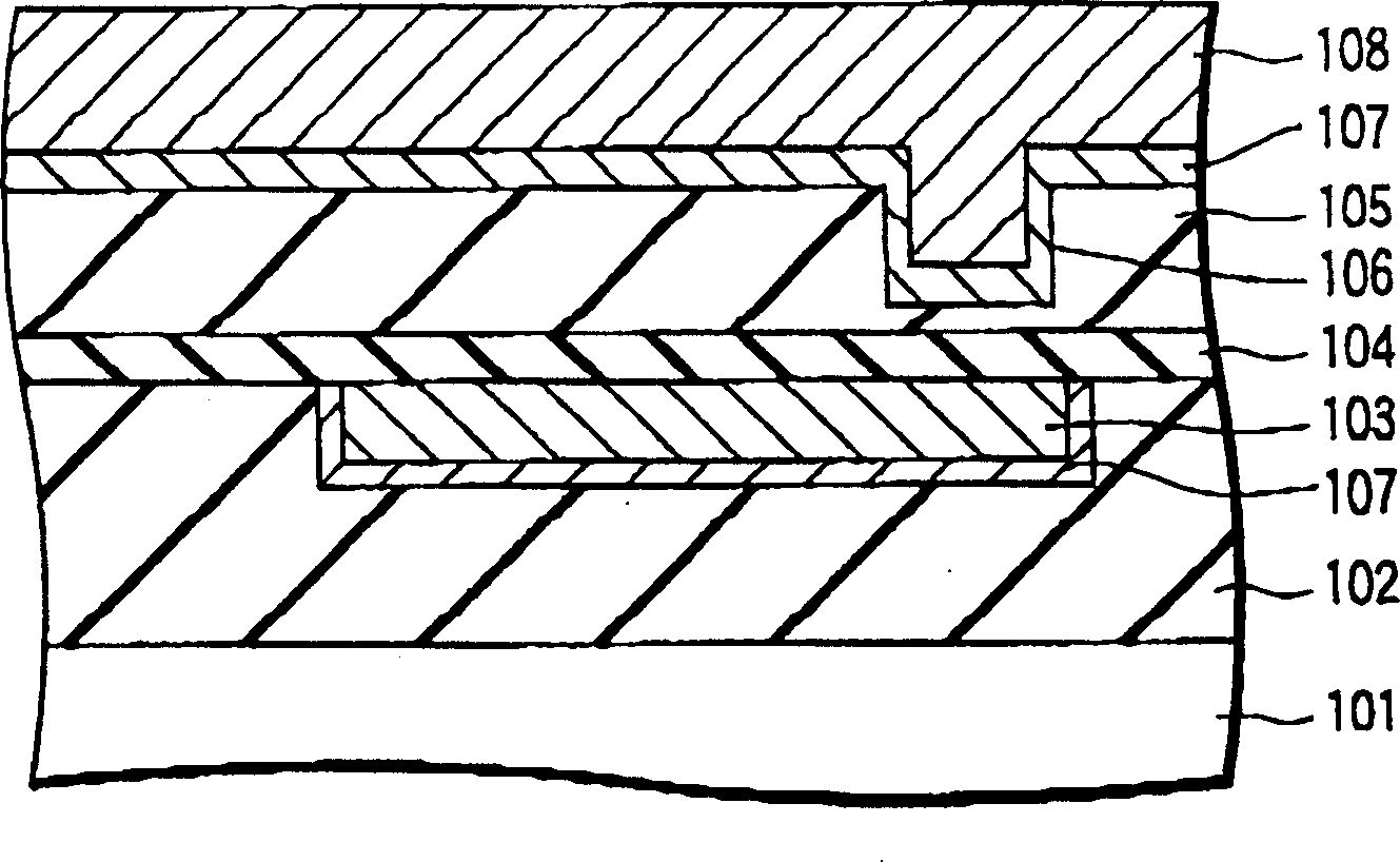
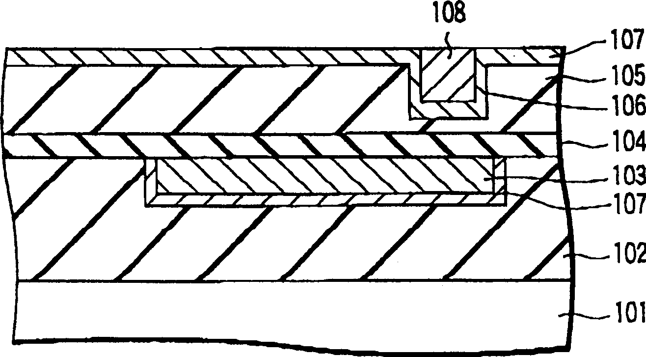
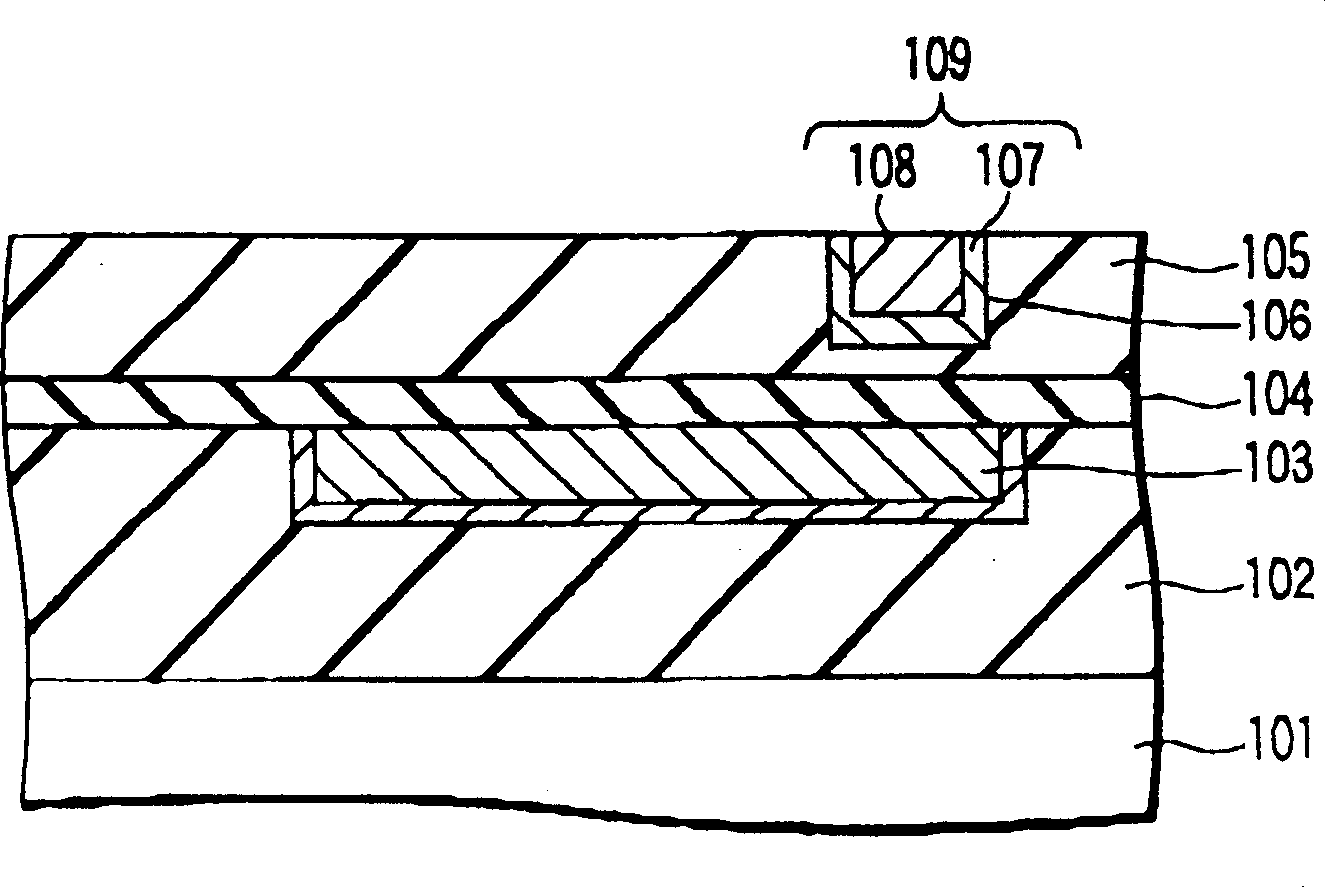
[0042] The formation of the Cu damascene wiring layered structure will now be described with reference to FIG. 1 . like Figure 1A As shown, an insulating film 102 is formed on the surface of a semiconductor substrate 101 having an active element (not shown) formed therein. In addition, a Cu buried wiring 103 is formed in the insulating film 102 while a tantalum nitride (TaN) liner film 107 is interposed between the Cu buried wiring 103 and the insulating film 102 . In addition, a silicon nitride (SiN) film 104 functioning as an interlayer insulating film and a silicon dioxide (SiO 2 ) film 105.

[0043] In the next step, a wiring groove 106 or hole (not shown) for forming a plug for conductively connecting the lower wiring layer to the upper wiring layer is formed in the interlayer insulating film 105. Next, a layered structure of a tantalum nitride (TaN) liner film 107 and a copper (Cu) film 108 is formed in such a manner as to fill up the wiring groove 106 . After formi...

example 2

[0061] The embodiment of Example 2 is directed to an example in which reflectance is measured in situ during CMP processing of a Cu film included in a wafer identical in construction to the wafer in Example 1, that is, the wafer is fabricated so that the multilayer The film is stacked on a semiconductor substrate.

[0062] For this method, the Figures 6A-6C CMP apparatus with the configuration shown. Specifically, Figure 6A is a perspective view showing the structure of the CMP apparatus, Figure 6B Yes Figure 6A Plan view of the CMP apparatus shown in , and Figure 6C Yes Figure 6A Side sectional view of the left part of the CMP apparatus shown in .

[0063] The CMP apparatus was constructed as follows. Specifically, a polishing pad 603 is mounted on a turntable 601, and a wafer 605 supported by a carrier 607 is mounted such that the surface of the wafer 605 to be polished faces downward. A slurry supply nozzle 609 is installed above the polishing pad 603 so that ...

example 3

[0067] This example is for the formation of aluminum pads on copper (Cu) damascene wiring, such as Figures 7A-7C shown. As shown in each figure, copper (Cu) buried wiring 703 is formed in an insulating film 702 on a semiconductor substrate 701 having active elements (not shown) formed therein. In addition, a tantalum nitride (TaN) liner film 700 is interposed between the copper buried wiring 703 and the insulating film 702 . In addition, silicon nitride (SiN) film 704 and silicon dioxide (SiO 2 ) film 705 is sequentially formed on the product structure, followed by patterning on the interlayer insulating film 705 to form a hole 706.

[0068] In the next step, a tantalum (Ta) film 707 as a barrier metal layer and an aluminum (Al) film 708 are formed on the interlayer insulating film 705 in such a manner as to fill up the holes 706 . Then, a resist film is formed on the entire surface, and then the resist film is patterned so that the resist film 709 remains in the portion w...


PUM

PropertyMeasurementUnit
thicknessaaaaaaaaaa
thicknessaaaaaaaaaa
thicknessaaaaaaaaaa

Abstract

A method for judging the residual film on a sample by optical measurement, the sample includes a first metal film and an insulating film, the change of the reflectance of the first metal film depends on the wavelength of the measurement light, and the insulating film is on the first metal film Formed above, the residual film is a second metal film above the insulating film, the method includes: irradiating the sample with measuring light, so as to measure the change of the intensity of light reflected from the sample as the wavelength of the measuring light changes, thereby obtaining a reflectance spectrum curve ; and dividing the reflectance spectral curve into several wavelength regions, so as to judge whether there is a second metal film above the insulating film according to the waveform in each spectral region of the reflectance spectral curve.

Description

[0001] Cross References to Related Applications [0002] This application is based on and claims the benefit of priority from prior Japanese Patent Application No. 2002-89772 filed on March 27, 2002, the entire contents of which are hereby incorporated by reference. technical field [0003] The invention relates to a method for judging a residual film by optical measurement, in particular to a method for judging a residual film by using a spectral reflection interferometer in an inspection step in a semiconductor device manufacturing process. Background technique [0004] In the traditional method of measuring film thickness using a spectral reflectance interferometer, a fit is made between the measured reflectance spectrum and the reflectance spectrum calculated from a predicted model of the laminated film in order to determine the film thickness, thus Determine the layered structure of the sample. However, in the conventional method, if the structure of the film to be mea...

Claims


Application Information

Patent Timeline
Patent Type & Authority Applications(China)
IPC IPC(8): G01N21/27G01N21/84G01R31/265H01L21/304H01L21/3205H01L21/66H01L21/768
CPCG01N21/55G01N21/8422G01R31/2656H01L22/12H01L22/00
Inventor 窪田壮男重田厚
Owner KK TOSHIBA
Why Eureka
Try Eureka