Supercharge Your Innovation With Domain-Expert AI Agents!

Apparatus and method for programming virtual ground nonvolatile memory cell array without disturbing adjacent cells

A technology of virtual grounding and non-volatile storage, applied in the field of semiconductor memory devices, which can solve the problems of increasing the overall size of semiconductor memory chips, wasting space, increasing space and cost, etc.

Inactive Publication Date: 2003-10-15
MACRONIX INT CO LTD
View PDF0 Cites 9 Cited by
  • Summary
  • Abstract
  • Description
  • Claims
  • Application Information

AI Technical Summary

Problems solved by technology

However, these conventional designs are space-consuming and inefficient
These designs will lead to a huge increase in the overall size of the semiconductor memory chip, so that the occupied space and cost are excessively increased.

Method used


Image

  • Apparatus and method for programming virtual ground nonvolatile memory cell array without disturbing adjacent cells
  • Apparatus and method for programming virtual ground nonvolatile memory cell array without disturbing adjacent cells
  • Apparatus and method for programming virtual ground nonvolatile memory cell array without disturbing adjacent cells

Examples


Embodiment Construction

[0024] The following description is presented to enable any person skilled in the art to make and use the invention. Various modifications to the disclosed embodiments will be readily apparent to those skilled in the art, and the general principles defined herein can be applied to other embodiments and applications without departing from the spirit and scope of the invention . Thus, the present invention is not limited to the shown embodiments, but is to be accorded the widest scope consistent with the principles and features disclosed herein.

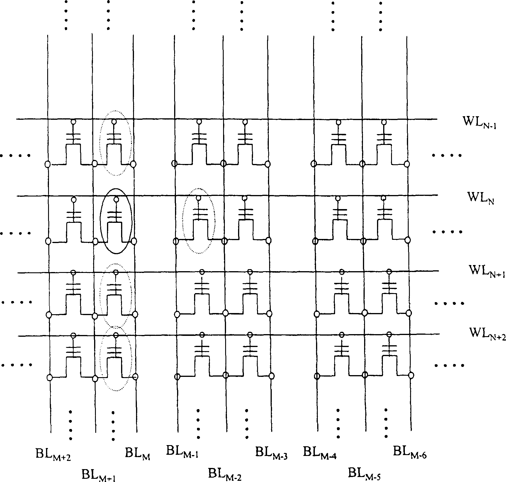
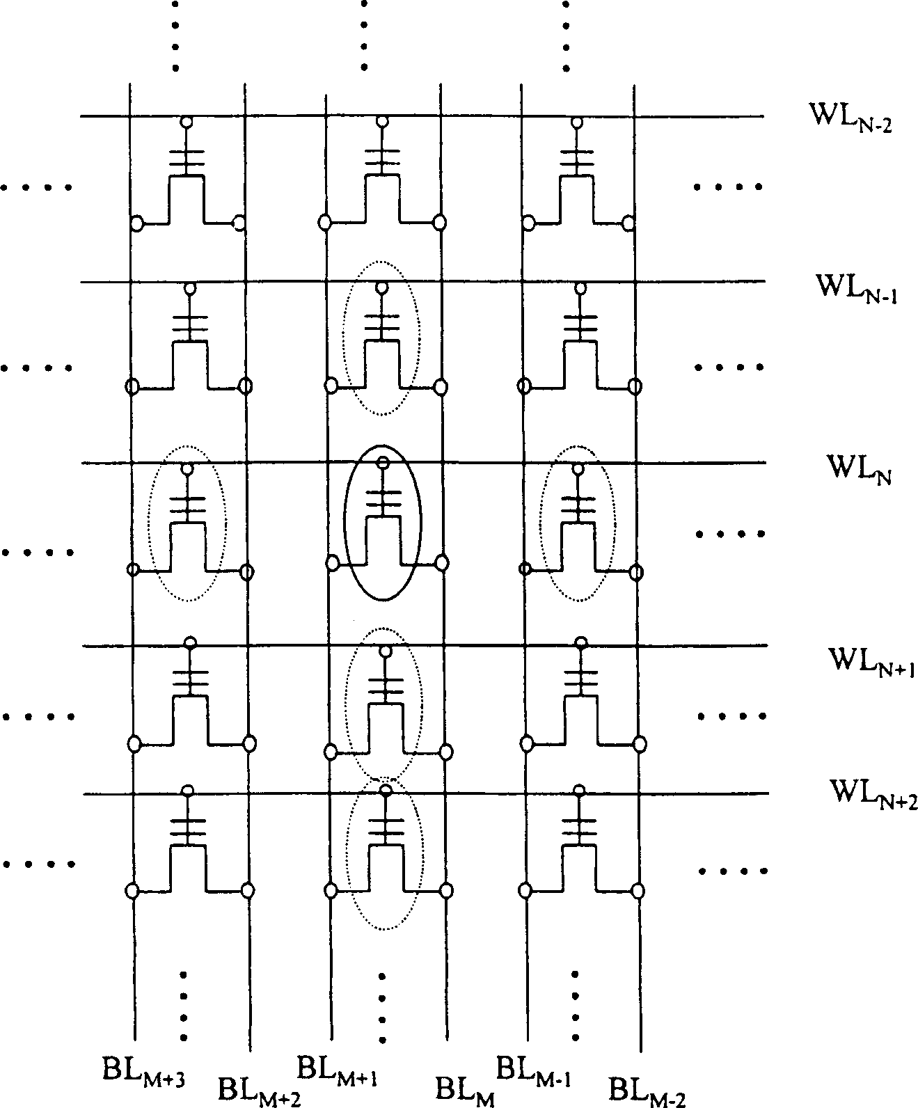
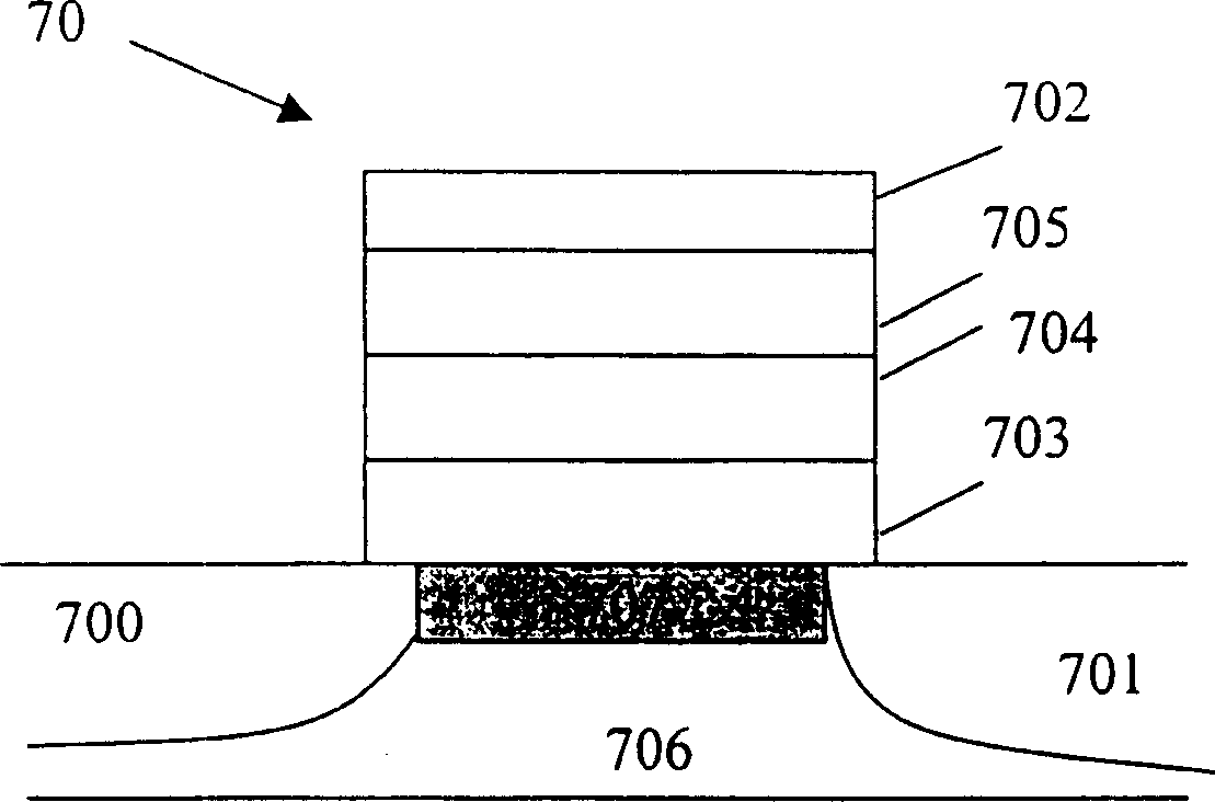
[0025] A nonvolatile memory unit 80 according to an embodiment of the present invention is illustrated in Figure 4 middle. The non-volatile memory cell 80 generally includes an N-channel metal oxide semiconductor field effect transistor (MOSFET) structure. In the nonvolatile memory cell 80 , a p-type substrate 806 includes two embedded N+ junctions, one of which is the source 800 and the other is the drain 801 . A channel region 80...


PUM


Abstract

The virtually earthing non-volatile memory unit array is formed with several adjacent non-volatile memory units arranged into array with several rows and lines. Each of the non-volatile memory unit is formed with one N-channel MOSFET with trapping layer between two insulating layers. In erasing state, certain amount of electrons is stored in the trapping layer. The programming method of the virtually earthing non-volatile memory array is also revealed. The potential applied to the bit line and the character line are preset to program the non-volatile memory unit without disturbing the adjacent non-volatile memory units to be programmed.

Description

technical field [0001] The invention relates to a semiconductor memory device, in particular to a method and a device for programming a virtually grounded nonvolatile memory cell array without disturbing adjacent cells. Background technique [0002] FIG. 3 is a block diagram illustrating the structure of a nonvolatile memory cell in the prior art, wherein a nonvolatile memory cell 70 includes an N-channel MOSFET (Metal Oxide Semiconductor Field Effect Transistor) structure. The non-volatile memory unit 70 includes a P-type substrate 706 with two embedded N+ junctions, one is a source 700 and the other is a drain 701 . A channel region 707 is formed between the source 700 and the drain 701 . Above the channel is a first insulating layer 703, typically a silicon oxide layer. On top of the first insulating layer 703 is a trapping layer 704, which is typically a nitride layer. The trapping layer 704 forms a memory retention layer that traps electrons as they are injected into...

Claims


Application Information

Patent Timeline
IPC IPC(8): G11C16/04G11C16/12
CPCG11C16/12G11C16/0491
Inventor 叶致锴蔡文哲卢道政
Owner MACRONIX INT CO LTD
Features
  • R&D
  • Intellectual Property
  • Life Sciences
  • Materials
  • Tech Scout
  • Unparalleled Data Quality
  • Higher Quality Content
  • 60% Fewer Hallucinations
Learn More