Transient-inhibiting audio-frequency circuit and method
A circuit and audio signal technology, applied in electrical components, low-frequency amplifiers, amplifiers with semiconductor devices/discharge tubes, etc., can solve problems such as click sound, working channel crosstalk, etc. Effects of offset or distortion, subtracted transients
- Summary
- Abstract
- Description
- Claims
- Application Information
AI Technical Summary
Problems solved by technology
Method used
Image

Examples
Embodiment Construction
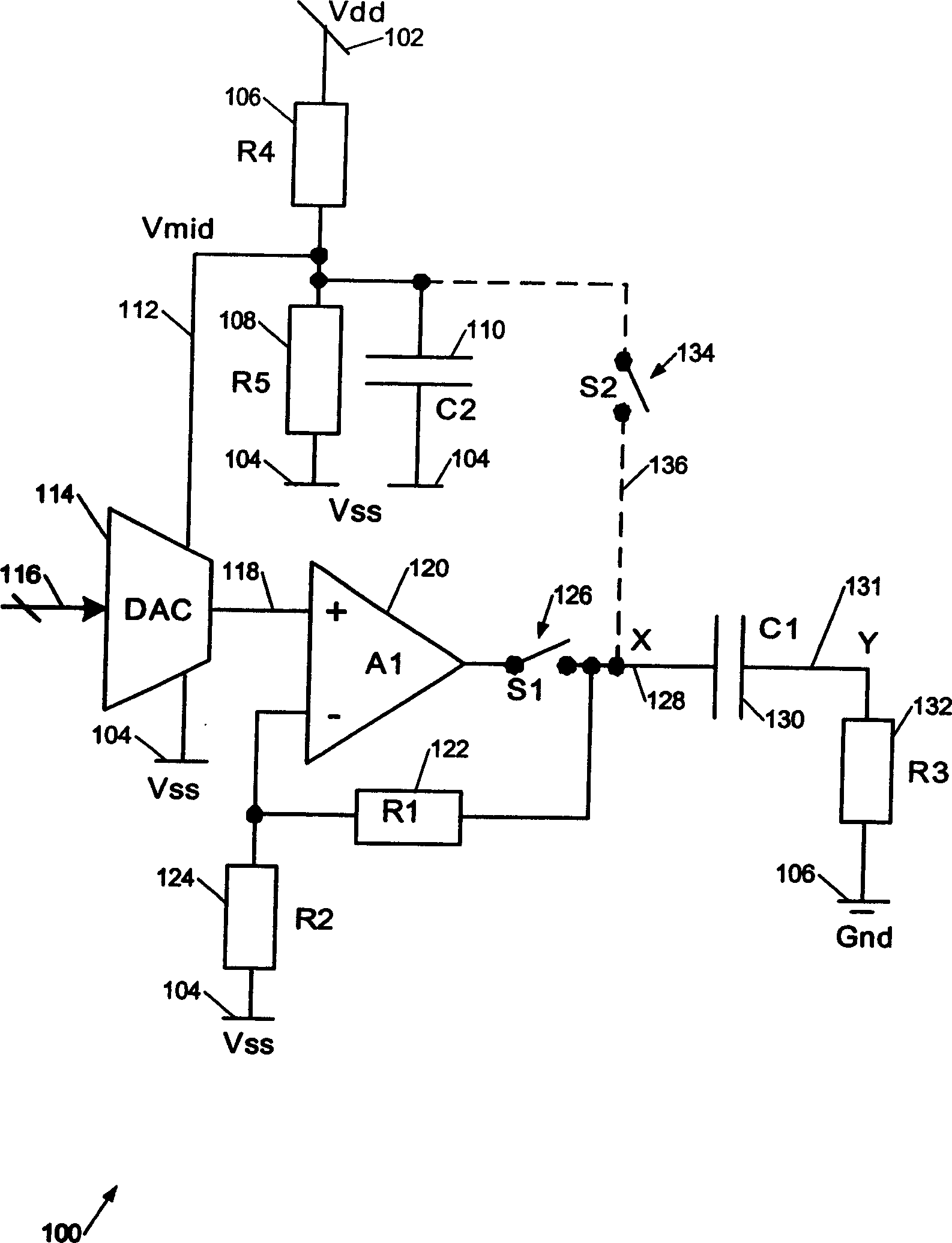
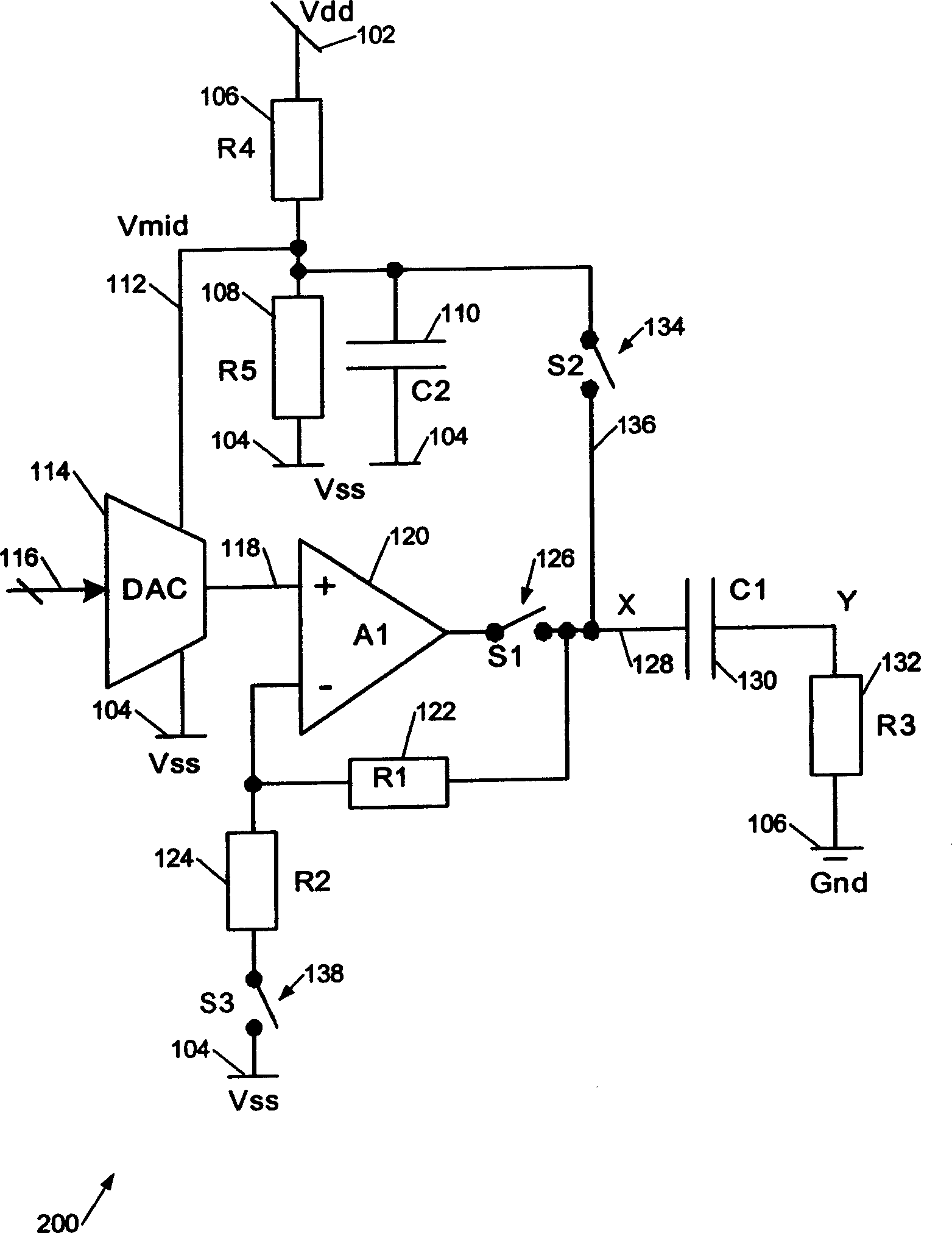
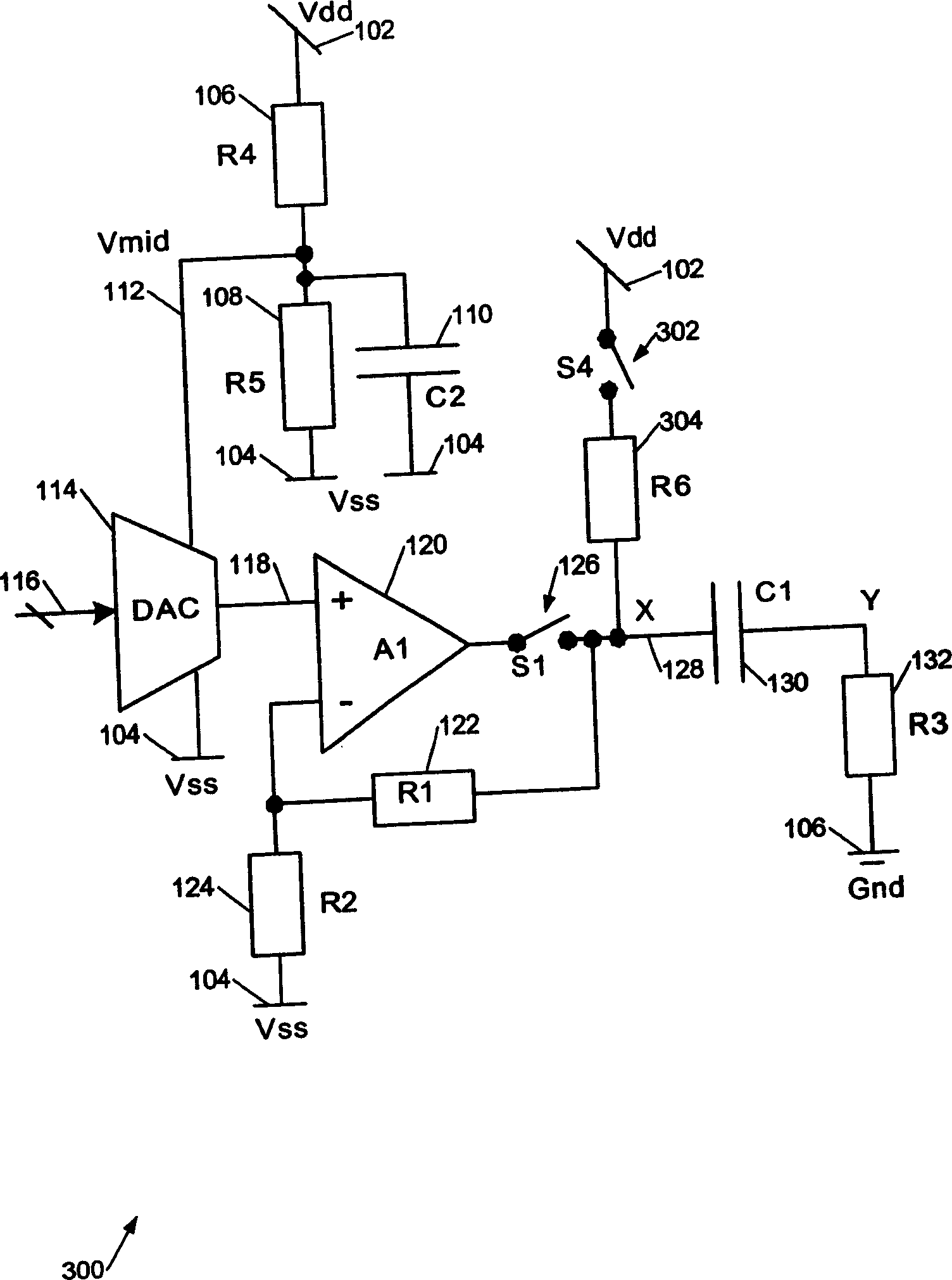
[0046] In general, in an example of the invention, the output of an amplifier or buffer (or output of a filter or other signal processing circuit) in the circuit is disconnected from the circuit in standby mode. Although in general the output node voltage of the circuit will be pulled to the main power supply voltage (for example, pulled down) by one or more resistance elements in the circuit, due to the addition of elements matching these resistance elements in the design of the present invention , so the output node voltage is pulled back to a quiescent voltage or a non-signal voltage. The resistive elements that pull the output voltage to the main supply voltage are usually elements of the feedback circuit, which may be one or more resistors; the matching elements to these resistive elements are preferably matched resistors, and those experienced in the industry will understand what is said here The "matched" does not necessarily mean "equal", but refers to using matched re...
PUM
 Abstract
Description
Claims
Application Information
 - Generate Ideas
- Intellectual Property
- Life Sciences
- Materials
- Tech Scout
- Unparalleled Data Quality
- Higher Quality Content
- 60% Fewer Hallucinations
Browse by: Latest US Patents, China's latest patents, Technical Efficacy Thesaurus, Application Domain, Technology Topic, Popular Technical Reports.
© 2025 PatSnap. All rights reserved.Legal|Privacy policy|Modern Slavery Act Transparency Statement|Sitemap|About US| Contact US: help@patsnap.com