IC device and its manufacture

A technology of integrated circuits and semiconductors, applied in circuits, semiconductor/solid-state device manufacturing, electrical components, etc., to solve problems such as failure to provide protection and damage to memory cells

Inactive Publication Date: 2004-01-21
MACRONIX INT CO LTD
View PDF1 Cites 69 Cited by
  • Summary
  • Abstract
  • Description
  • Claims
  • Application Information

AI Technical Summary

Problems solved by technology

However, this combination does not provide sufficient protection as the memory cell will be damaged before reaching the junction breakdown potential

Method used


Image

  • IC device and its manufacture
  • IC device and its manufacture
  • IC device and its manufacture

Examples


Embodiment Construction

[0041] The following fit Figure 4 to Figure 6 Embodiments of the present invention will be described. First, please refer to Figure 4 , which shows an integrated circuit device 10 including a protection circuit according to the present invention. The integrated circuit device 10 includes a device substrate 11 . The integrated circuits 12 on the device substrate 10 perform "task" operations on the device 10 . "Task" operations include providing memory, logic functions, processing program functions, or any function provided by an integrated circuit.

[0042] A power supply provides a power voltage VCC and a reference ground to the device substrate 11 . The voltage generator circuit 13 on the device substrate 11 provides the integrated circuit 12 with operating voltages, including providing a node 14 with a low operating voltage and a high operating voltage.

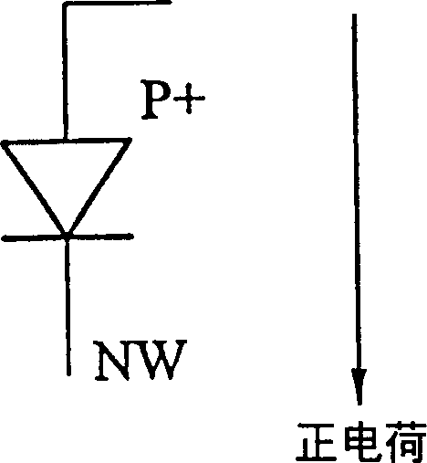
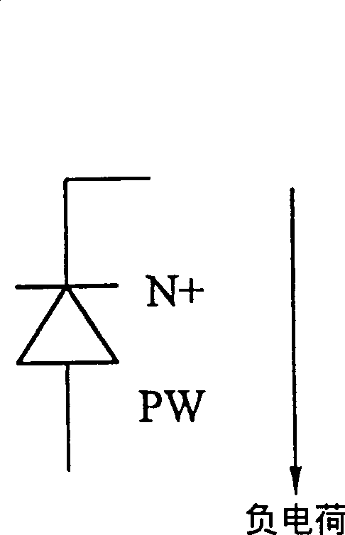
[0043] The protection device on the device substrate 10 includes a PMOS transistor 15 and an NMOS transistor 16 . ...


PUM


Abstract

The present invention relates to one kind of protection device and IC manufacturing process. The protection device includes one NMOS / PMOS pair with a dynamic initial voltage, and the NMOS and the PMOS have separate grids coupled to the semiconductor in the channel area. Cooperating with proper metal connection, the said structure can protect IC in manufacture from plasma and charge damage and protect IC in operation from abnormal voltage.

Description

technical field [0001] The present invention relates to an integrated circuit device and its manufacture, including the manufacture of a non-volatile (non-volatile) storage device, in particular to a protective device for an integrated circuit and its manufacturing process, so that it is protected from plasma damage during manufacture . Background technique [0002] In the manufacture of integrated circuits, the production method of active ions is often used. For example, back-end fabrication involves metal etching, photoresist stripping, and deposition of inter-metal dielectric layers, where the plasma induces charges on the structures being processed. These plasmonic-induced charges can damage structures in underlying devices, including structures that seriously affect device performance. For example, tunneling dielectric layers, gate dielectric layers, and polysilicon interlayer dielectric layers used in flash memory devices are damaged by plasma-induced charges. Furth...

Claims


Application Information

Patent Timeline
Patent Type & Authority Applications(China)
IPC IPC(8): H01L21/8239H01L21/8246H01L21/8247H01L27/092
CPCH01L27/092H01L27/1052H01L27/11521H01L21/8239H01L27/11568H10B99/00H10B43/30H10B41/30
Inventor 周铭宏陈土顺黄俊仁
Owner MACRONIX INT CO LTD
Why Eureka
Try Eureka