Semiconductor module and method for mfg. semiconductor module

A semiconductor and circuit module technology, applied in semiconductor/solid-state device manufacturing, semiconductor devices, semiconductor/solid-state device components, etc., can solve problems such as low component density

Inactive Publication Date: 2004-02-25
INFINEON TECH AG
View PDF0 Cites 21 Cited by
  • Summary
  • Abstract
  • Description
  • Claims
  • Application Information

AI Technical Summary

Problems solved by technology

Therefore, such an arrangement with a commonly used arrangement has a large overall thickness in the case of a single-sided layout, at least d1+d2+d3, which will lead to a module thickness of more than 2mm, which in turn, leads to a low component density, the main reason are interposer substrates and conductive tracks with large area requirements

Method used


Image

  • Semiconductor module and method for mfg. semiconductor module
  • Semiconductor module and method for mfg. semiconductor module
  • Semiconductor module and method for mfg. semiconductor module

Examples


Embodiment Construction

[0048] In the drawings, the same reference numerals represent the same or functionally same components.

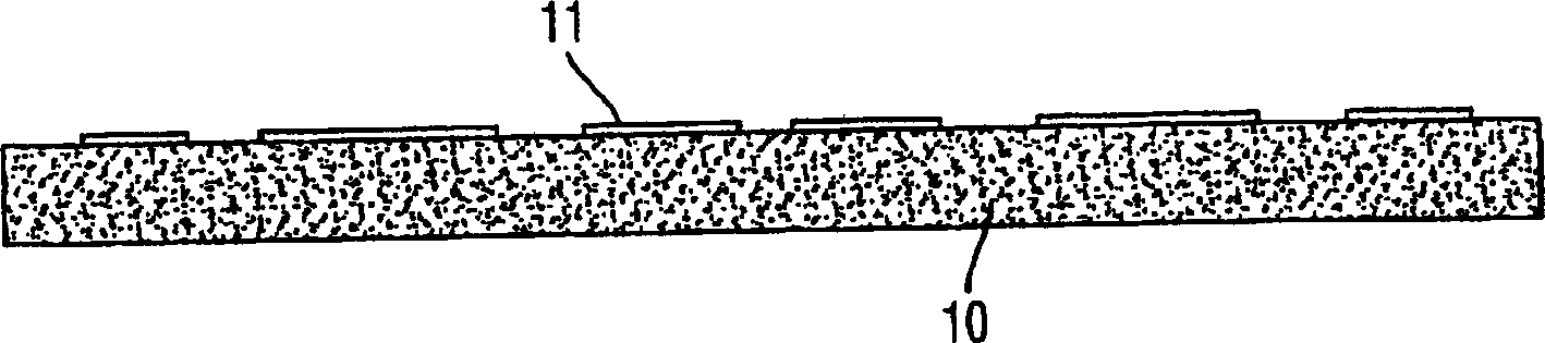
[0049] Figure 1A A transfer substrate 10 is shown, for example made of glass, metal, or polymer, to which a patterned dielectric connection plane 11 is applied in a printing process. The dielectric connection plane 11 is not cured at the time it is being talked about at this time, and is still tacky. The dielectric connection plane 11 comprises, for example, polymer, epoxy, adhesive, silicone, or polyimide.

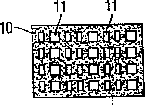
[0050] Figure 1B In plan view a transfer substrate 10 is shown, on which the individual connection regions 11 of a dielectric connection plane 11 are applied, the transfer substrate being made in the form of a rectangle.

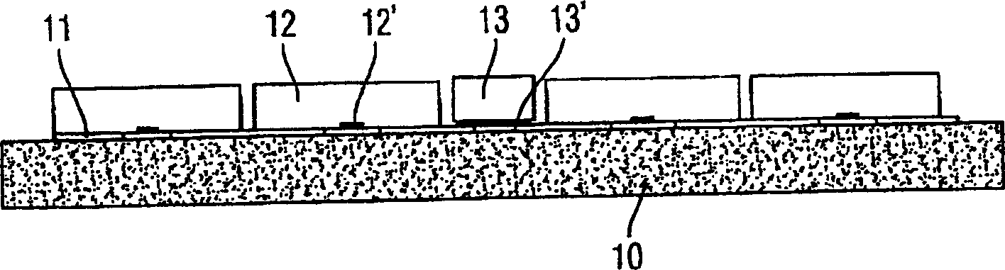
[0051] exist Figure 2A In the embodiment, active circuit devices 12 and passive circuit devices 13 are added to the transfer substrate 10 and the patterned connection plane 11. The circuit devices 12, 13 are added to the predetermined positi...


PUM


Abstract

Production of a semiconductor module (31) comprises: (a) applying a structured connecting layer (11) on a supporting substrate; (b) applying active switching units (12) and / or passive switching units (13) with contact surfaces (12', 13') pointing to a transfer substrate on the structured connecting layer; (c) connecting the switching units with each other using a filler (14) between the units; (d) removing the transfer substrate; and (e) applying electrical connecting units (16) to selectively contact the contact surfaces of the switching units. An Independent claim is also included for a semiconductor module produced by the above process.

Description

technical field [0001] The invention relates to a semiconductor module and a method for manufacturing the semiconductor module. Background technique [0002] Semiconductor modules such as those used in computer systems or memory devices of computer systems generally constitute a module form. A conventional memory module must have two main sets of components. One is active or passive circuit components, and the other is a printed circuit board. The printed circuit board serves as a carrier for circuit components, provides connection elements such as conductive tracks, and makes connections to the outside. [0003] Active circuit devices, such as memory chips, are individual packaged chips. The following functions are implemented in this package: connection between the contacts of the chip to form a type of rewiring (lead frame, interposer). This may be done through a bonding process or through small solder beads, the internal connection elements. This rewiring serves as ...

Claims


Application Information

Patent Timeline
Patent Type & Authority Applications(China)
IPC IPC(8): H01L21/60H01L21/68H01L21/98H01L23/538
CPCH01L2924/15311H01L2924/01005H01L2924/01082H01L2224/73204H01L2924/01039H01L2924/12044H01L24/96H01L2224/32225H01L2224/24195H01L2924/01015H01L25/50H01L2224/24137H01L2924/014H01L24/82H01L24/24H01L2924/01029H01L2224/16225H01L2924/19043H01L2924/01078H01L2924/01006H01L21/6835H01L2924/01033H01L21/568H01L23/5389H01L2924/19041H01L2924/01079H01L2224/05568H01L2224/05573H01L2924/00014H01L2924/07802H01L2924/00H01L2224/05599
Inventor 格尔德·弗兰科夫斯克基哈丽·黑德勒芭芭拉·瓦斯克斯
Owner INFINEON TECH AG
Why Eureka
Try Eureka