Interconnection structure containing stress regulating covering and its mfg. method

A technology of interconnect structure and stress adjustment, which can be used in semiconductor/solid-state device manufacturing, semiconductor/solid-state device components, semiconductor devices, etc., and can solve problems such as poor adhesion

Inactive Publication Date: 2004-02-25
格芯公司
View PDF1 Cites 6 Cited by
  • Summary
  • Abstract
  • Description
  • Claims
  • Application Information

AI Technical Summary

Problems solved by technology

[0005] Another problem associated with these existing structures is the poor adhesion observed at

Method used


Image

  • Interconnection structure containing stress regulating covering and its mfg. method
  • Interconnection structure containing stress regulating covering and its mfg. method
  • Interconnection structure containing stress regulating covering and its mfg. method

Examples


Embodiment Construction

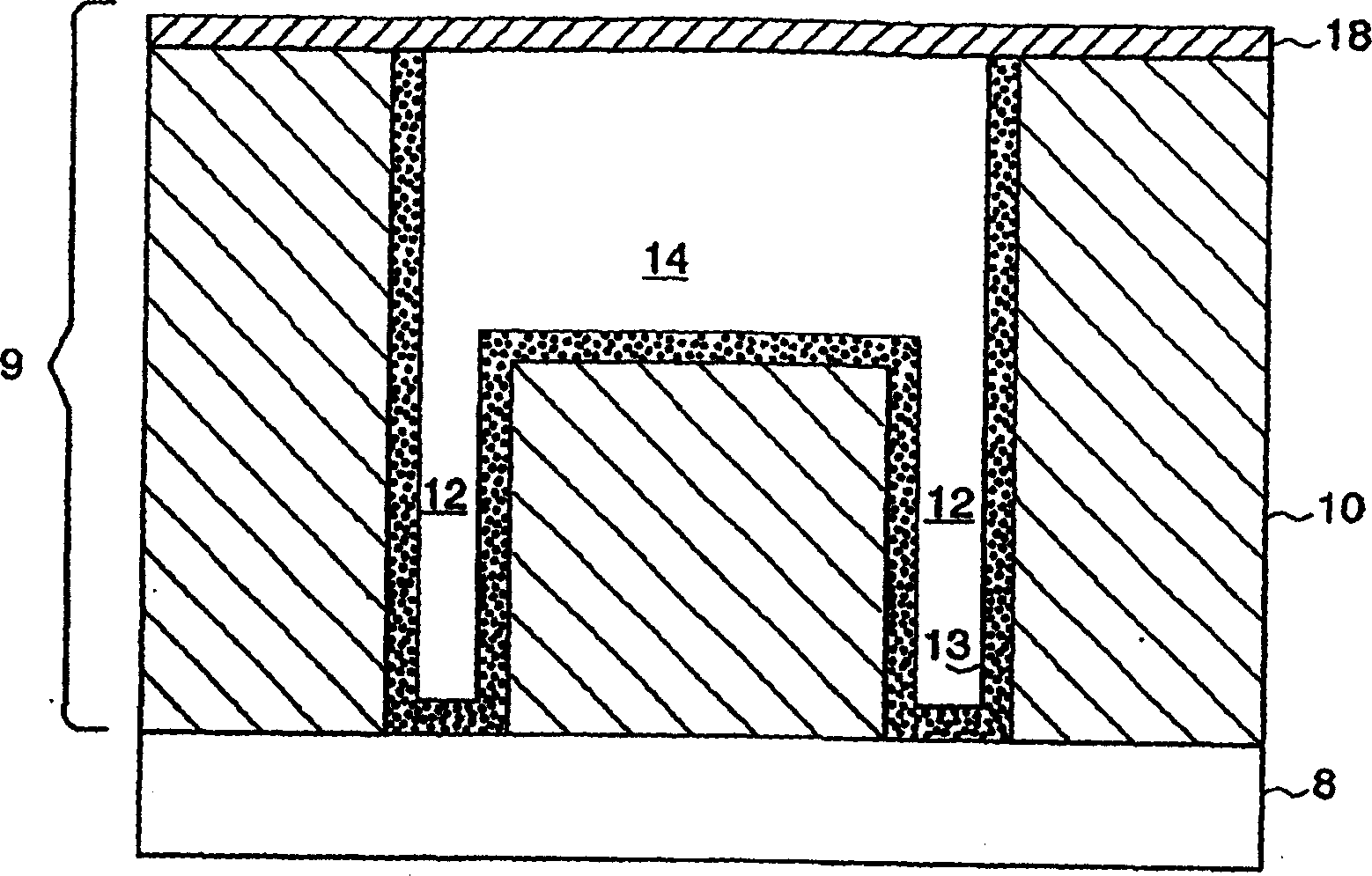
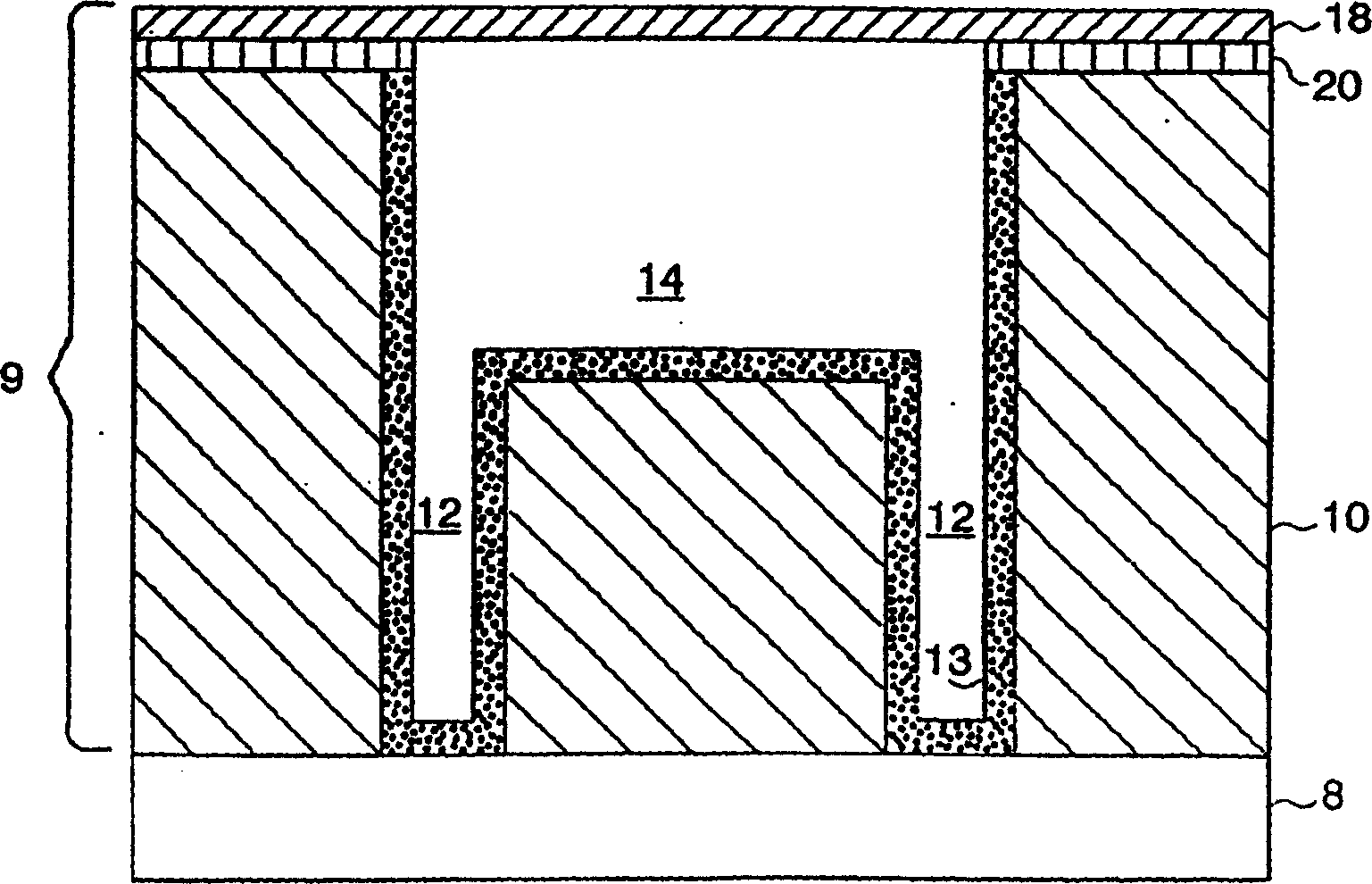
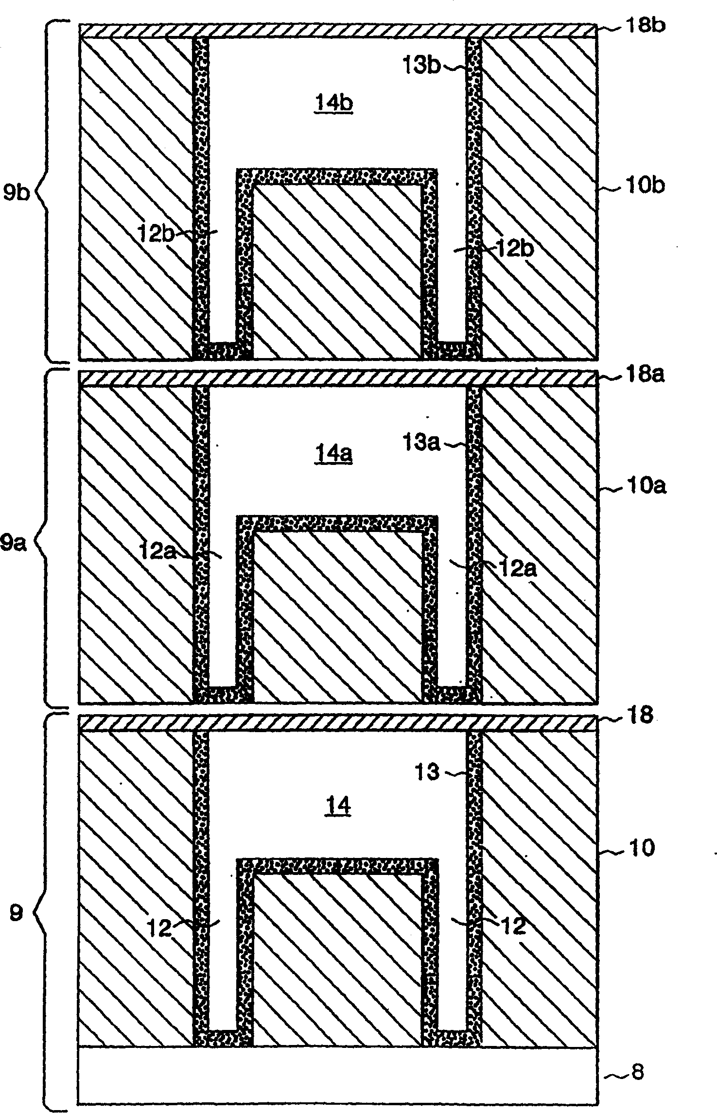
[0024] The present invention is directed to an interconnection structure for forming a semiconductor device, by employing a stress-regulating capping layer between a first layer having an associated first internal stress and a second layer having an associated second internal stress, the The interconnect structure has greatly reduced internal stress. Typically, the first internal stress associated with the first layer is a tensile stress, and the second internal stress associated with the second layer is either tensile or compressive, depending on the particular material selected for the second layer. The interconnection structure of the present invention is based on the surprising discovery that when specific materials are chosen for the first and second levels, the stresses of the respective materials enable stress modulation with an associated specific stress (i.e., tensile or compressive stress). Covering materials can be chosen to substantially reduce the overall internal...


PUM

PropertyMeasurementUnit
Thermal expansion coefficientaaaaaaaaaa

Abstract

Novel interconnect structures possessing a relatively low internal stress and dielectric constant for use in semiconductor devices are provided herein. The novel interconnect structures comprise a first layer having a coefficient of thermal expansion greater than about 20 ppm and a first internal stress associated therewith, the first layer having a first set of metallic lines formed therein; a second layer having a coefficient of thermal expansion less than about 20 ppm and a second internal stress associated therewith, the second layer having a second set of metallic lines formed therein; and one or more stress adjustment cap layers formed between the first layer and the second layer, the cap layer(s) having a third internal stress to offset the first stress of the first layer and the second stress of the second layer and inducing a favorable relief of stress on the interconnect structure. Methods for making a semiconductor device having a substantially reduced internal stress are also provided.

Description

technical field [0001] The present invention relates generally to integrated circuits (ICs), and more particularly to interconnect structures, including multilayer interconnect structures, in which the internal stress of the structure is substantially reduced through the use of a stress regulating capping layer. The invention also relates to a method of fabricating an interconnect structure with greatly reduced internal stress. Background technique [0002] Typically, a semiconductor device includes multiple circuits forming an integrated circuit, including a chip (eg, a chip back end of line, or "BEOL"), a thin film package, and a printed circuit board. Integrated circuits are used in computers and electronic equipment and can contain millions of transistors and other circuit elements fabricated on a single crystal silicon substrate. In order for the device to work, a complex network of signal paths is usually provided to connect circuit elements distributed over the surfa...

Claims


Application Information

Patent Timeline
IPC IPC(8): H01L21/768H01L23/522H01L23/532
CPCH01L23/53295H01L23/5329H01L2924/0002H01L2924/00H01L21/768
Inventor 斯蒂芬·M·盖茨蒂莫西·J·多尔顿约翰·A·费兹西门斯
Owner 格芯公司
Why Eureka
Try Eureka