Thin film magnetic memory device suppressing resistance of transistors present in current path

A technology of magnetic body and transistor, applied in the field of thin film magnetic body memory, can solve the problems of time-consuming read operation, wrong reading, and obstacles to high-speed data reading, and achieve high-speed pre-charging operation, lightening RC load, and high-speed data. The effect of reading

Inactive Publication Date: 2004-03-17
MITSUBISHI ELECTRIC CORP
View PDF0 Cites 2 Cited by
  • Summary
  • Abstract
  • Description
  • Claims
  • Application Information

AI Technical Summary

Problems solved by technology

Therefore, if the resistance of the transistor group becomes large, the read current does not necessarily reflect the resistance of the selected memory cell, and there is a risk of erroneous reading.
In addition, due to the influence of the resistance of the transistor group, it takes time to read the operation, and there is a danger of hindering the speed-up of data reading.

Method used


Image

  • Thin film magnetic memory device suppressing resistance of transistors present in current path
  • Thin film magnetic memory device suppressing resistance of transistors present in current path
  • Thin film magnetic memory device suppressing resistance of transistors present in current path

Examples


Embodiment 1

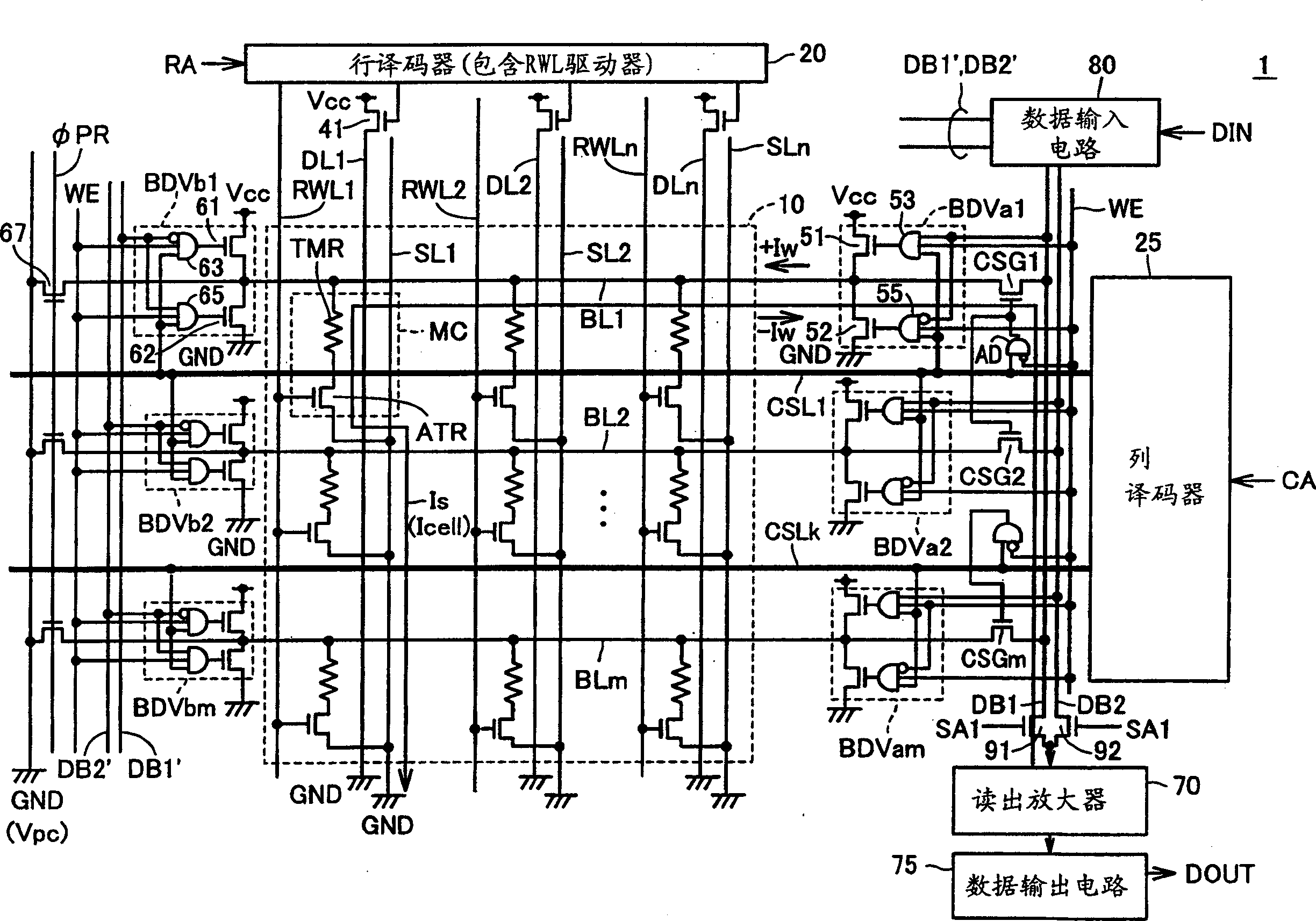
[0060] refer to figure 1 , the MRAM device 1 of embodiment 1 has: memory cell array 10, is formed by a plurality of MTJ memory cells MC that are arranged in n row * m column (n, m: natural number); Row decoder 20, performs according to row address RA row selection in the memory cell array 10; and a column decoder 25 for performing column selection in the memory cell array 10 according to the column address CA.

[0061] In memory cell array 10, read word lines RWL1-RWLn, digit lines DL1-DLn, and source voltage lines SL1-SLn are arranged corresponding to memory cell rows, and bit lines BL1-BLm are provided corresponding to memory cell columns. Hereinafter, read word lines RWL1 to RWLn, digit lines DL1 to DLn, bit lines BL1 to BLm, and source voltage lines SL1 to SLn are collectively referred to as read word lines RWL, digit lines DL, and bit lines BL, respectively. and source voltage line SL. In addition, the binary high voltage state (eg, power supply voltage Vcc) and low vo...

Embodiment 2

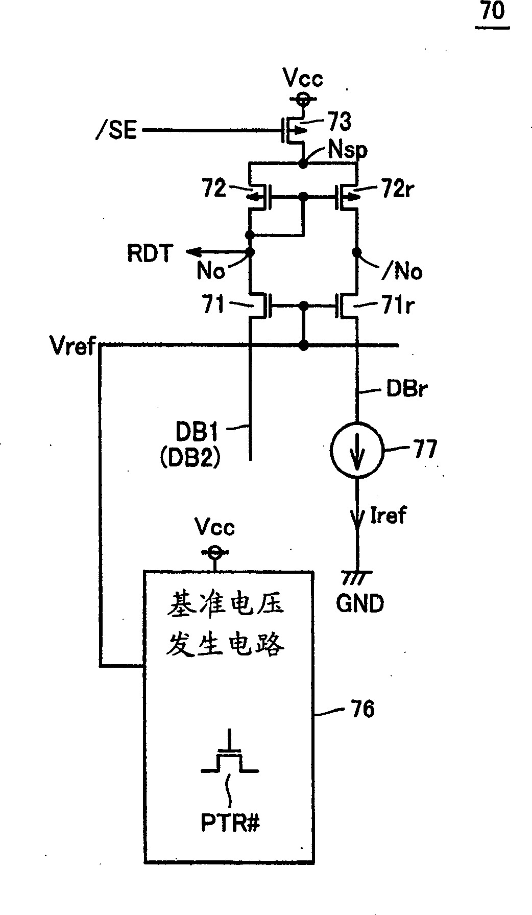
[0126] With reference to Fig. 7, the MRAM device 2 of embodiment 2 and according to figure 1 Compared with the MRAM device 1 of the embodiment shown in , there are differences in that read gate transistors RG1 to RGm are provided and that the connection structure between the bit line BL and the data bus lines DB1 and DB2 is different. In addition, there is a difference in that the sense amplifier circuit 70, which detects stored data based on the voltage or current present on the data bus DB1 or DB2, is replaced by the sense amplifier circuit 70#.

[0127] In the structure according to the second embodiment, the column selection gate transistors CSG1 to CSGm are electrically connected between the corresponding bit lines BL1 to BLm and the power supply voltage Vcc. In addition, regarding the on / off control of the column select gate transistors CSG1~CSGm, due to the figure 1are the same, so detailed description thereof will not be repeated.

[0128] Read gate transistors RG1...


PUM


Abstract

An access transistor ATR in an MTJ memory cell, which is one of transistors connected to a read current path, is constituted with a surface-channel, field-effect transistor. The surface-channel, field-effect transistor has a channel resistance lower than a channel-embedded, field-effect transistor, and can reduce an RC load in the read current path. Accordingly, data can be read with a high speed.

Description

technical field [0001] The present invention relates to a thin film magnetic memory, and more specifically, to a thin film magnetic memory including a magnetic memory cell having a magnetic tunnel junction (MTJ). Background technique [0002] As a new generation of nonvolatile memory, MRAM (Magnetic Random Access Memory) devices are attracting more and more attention. The MRAM device is a memory that stores nonvolatile data using a plurality of thin-film magnetic bodies formed on a semiconductor integrated circuit, and can perform random access to each of the thin-film magnetic bodies. [0003] In particular, it has been reported that in recent years, the performance of the MRAM device has been greatly improved by using a thin-film magnetic body utilizing a magnetic tunnel junction as a memory cell. [0004] Figure 8 is a schematic diagram showing the structure of a memory cell having a magnetic tunnel junction (hereinafter also simply referred to as an MTJ memory cell). ...

Claims


Application Information

Patent Timeline
Patent Type & Authority Applications(China)
IPC IPC(8): G11C11/15G11C11/16H01L21/8246H01L27/105H01L43/08
CPCG11C11/16
Inventor 日高秀人石川正敏大石司
Owner MITSUBISHI ELECTRIC CORP
Why Eureka
Try Eureka