Semiconductor laser device and solid laser device using same

A laser device and semiconductor technology, which is applied in the direction of semiconductor laser devices, semiconductor laser optical devices, semiconductor lasers, etc., can solve the problems that the end face excitation method of excitation efficiency cannot be used, and the parallel component is difficult to focus.

Inactive Publication Date: 2004-05-26
NIPPON STEEL CORP +1
View PDF1 Cites 17 Cited by
  • Summary
  • Abstract
  • Description
  • Claims
  • Application Information

AI Technical Summary

Problems solved by technology

[0019] However, as mentioned above, the stacked array semiconductor laser generating element uses a lens to converge the emitted light from the semiconductor laser generating element and focus it. The vertical component can be focused more easily. However, since the entire width of the light source is large, Therefore, it is difficult to focus the parallel component into a tiny light spot
[0020] If such a stacked array semiconductor laser is intended to be used as an excitation light source, as mentioned above, since the width of the array is within the range of 1 cm, it is impossible to use a common lens system to focus multiple beams into a single spot. , the end face excitation method with good excitation efficiency cannot be used, so it can only be used in the side excitation method

Method used


Image

  • Semiconductor laser device and solid laser device using same
  • Semiconductor laser device and solid laser device using same
  • Semiconductor laser device and solid laser device using same

Examples


Embodiment Construction

[0072] The present invention will be specifically described below according to the accompanying drawings.

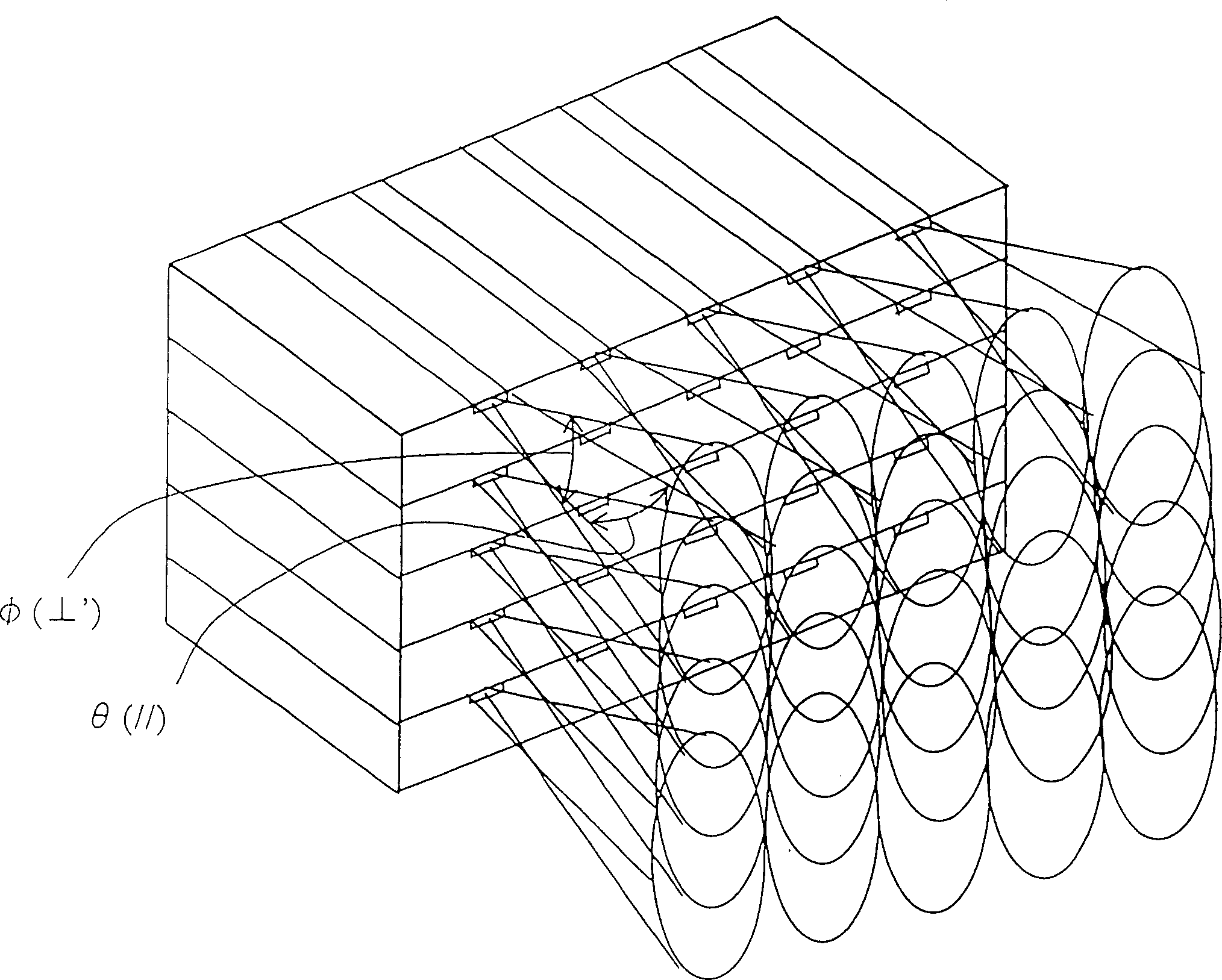
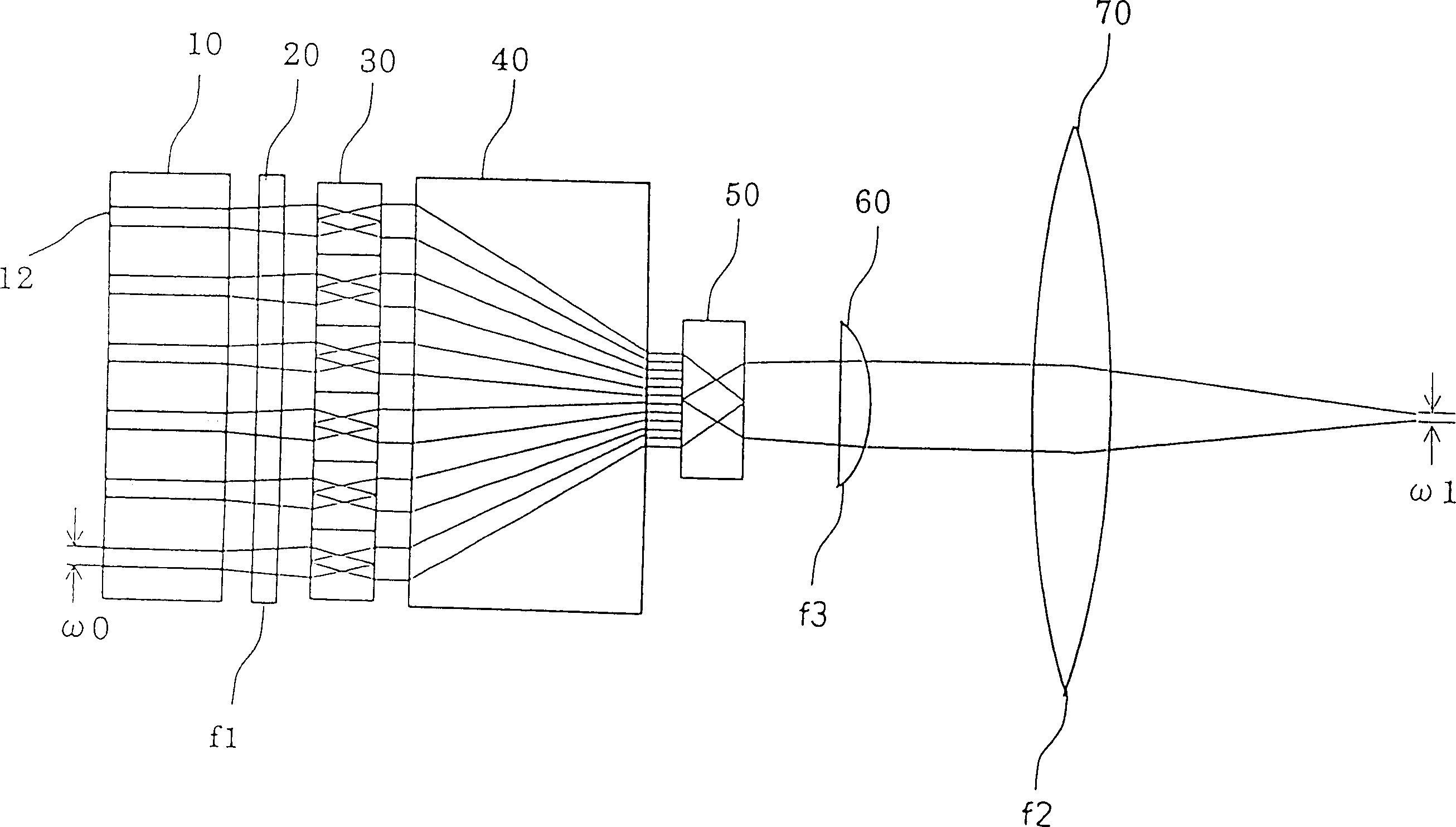
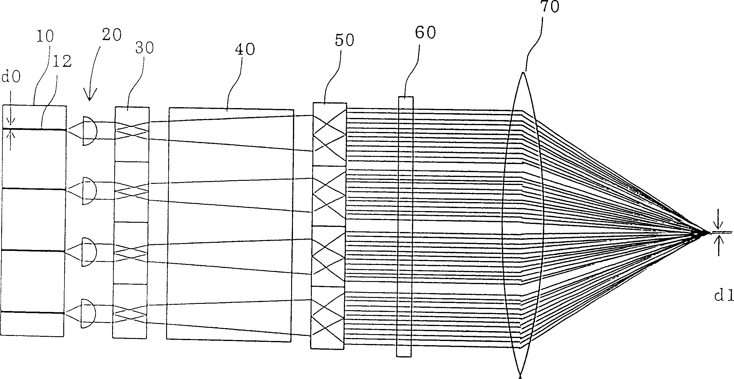
[0073] figure 2 is a plan view of the semiconductor laser device of the present invention, image 3 for its front view.

[0074] The stacked array semiconductor laser 10 is stacked with a linear array semiconductor laser (4 layers are shown in the figure) within a height range of 5 to 40 mm. In the linear array semiconductor laser, between intervals with a width of about 10 mm, 10 to 100 active layer strips 12 emitting laser beams (in the figure, 6 are shown for convenience) are arranged in a row.

[0075] In the cross-section of each active layer strip 12, for example, the width is in the range of 100-200 μm, and the thickness is in the range of 0.1-1 μm. The laser light emitted from the end face of the active layer strip constitutes the light emitting source of the stacked array semiconductor laser 10. , the radiation angle in the thickness direction is in the rang...


PUM


Abstract

A semiconductor laser device with the energy density increased at the focal point and a LD pumped solid-state laser device configured of the particular semiconductor laser device are provided. A stack array laser element for radiating a two-dimensional array of laser beams includes a plurality of parallel laser beam columns each aligned in the form of dotted lines. In front of the stack array laser element; each laser beam column collimated by being refracted in the direction substantially perpendicular to the direction of the dotted line is received, and radiated by turning at right angles to the direction of the laser beams from each emitter or emitter group. In this way, the laser beams are converted into a plurality of substantially ladder-shaped parallel laser beam columns. These parallel laser beam columns are compressed to form parallel laser beam columns in alignment. Each compressed one of parallel laser beam columns is turned at right angles and radiated. Thus, all the laser beams are converted into a plurality of aligned parallel laser beams, which are collimated and condensed at a focal point.

Description

technical field [0001] The invention relates to a beam converter for lamination array laser diodes and a laser device using the beam converter. The present invention also relates to a semiconductor laser light concentrator for converging semiconductor laser light into tiny light spots, and a semiconductor laser excitation solid-state laser device for optically exciting a solid-state laser device through semiconductor laser light. Background technique [0002] For laser processing, lasers for medical purposes use YAG (yttrium aluminum garnet). However, YAG, which is a solid-state laser, has low conversion efficiency from electricity to light. The reason is that due to the Xe lamp used for the excitation of solid-state lasers in the past, the luminous efficiency of the flash lamp is low. In addition, the luminous spectrum band is also wide, so only a small part of the luminous energy can be used for solid-state lasers. Laser excitation. This often necessitates the use of la...

Claims


Application Information

Patent Timeline
Patent Type & Authority Applications(China)
IPC IPC(8): G02B27/09H01S5/00H01S5/40
CPCH01S5/405G02B27/0972G02B19/0057G02B27/0966G02B27/0922H01S5/4025H01S5/4012G02B27/09H01S5/005G02B19/0014G02B27/0961G02B27/00
Inventor 山口哲滨田直也
Owner NIPPON STEEL CORP
Why Eureka
Try Eureka