Data latch time regulator

A technology for adjusting devices and data, which is applied in electrical digital data processing, static memory, memory systems, etc., to achieve the effect of easy design and suppressing the increase of circuit scale

Inactive Publication Date: 2004-06-09
PANASONIC CORP
View PDF1 Cites 6 Cited by
  • Summary
  • Abstract
  • Description
  • Claims
  • Application Information

AI Technical Summary

Problems solved by technology

As a result, there are a plurality of latch circuits and comparison circuits, and there is a disadvantage that a plurality of them need to be provided corresponding to the plurality of delay pulse signals.
This disadvantage is not limited to the latch timing of the read data from the memory, but also the latch timing of the data from the LSI

Method used


Image

  • Data latch time regulator
  • Data latch time regulator
  • Data latch time regulator

Examples


Embodiment 1

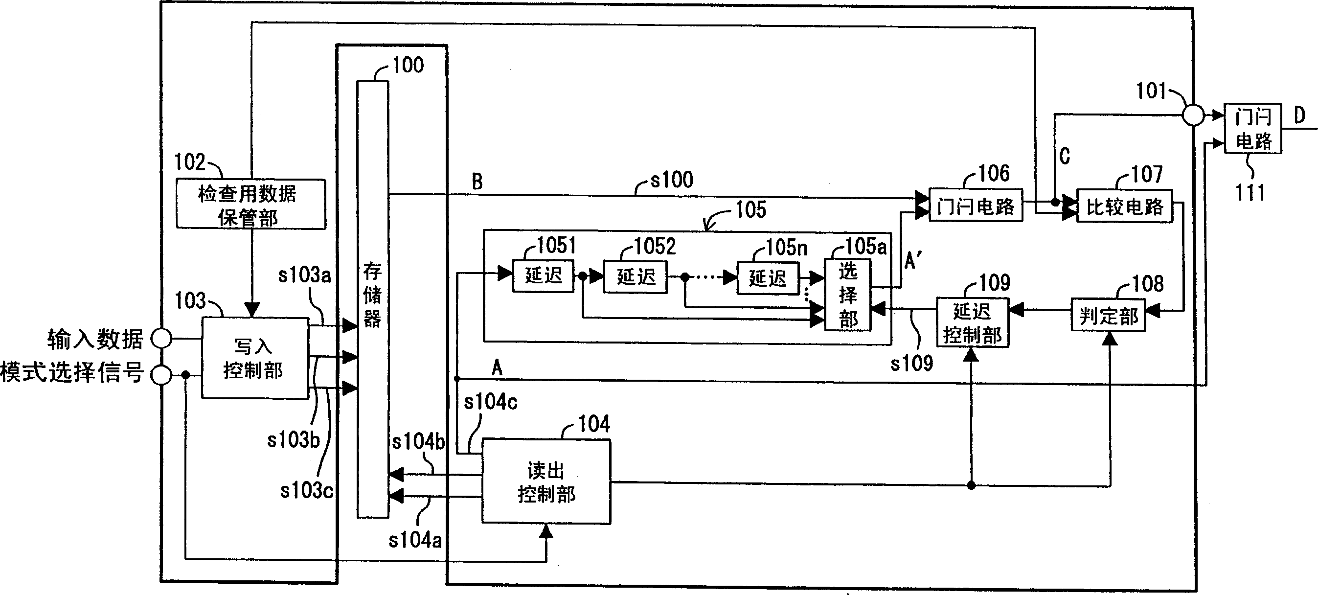
[0075] figure 1 A latch timing adjustment device according to Embodiment 1 of the present invention is shown. The adjusting device in the figure adjusts the latch timing of output data (read data) from the memory 100, and circuits other than the memory 100 and the latch circuit 111 are integrated into one LSI.

[0076] exist figure 1 Among them, 102 is an inspection data storage unit, which stores inspection data used when adjusting the latch timing of the read data from the memory 100 in advance. When multiple bits of inspection data are simultaneously read out from the memory 100 , the inspection data is stored in advance in a mode that takes into account interference between adjacent bits in the memory 100 , that is, crosstalk. For example, a bit for which the latch timing is adjusted is stored in consideration of whether signals adjacent to or adjacent to the bit change in the same phase and change in the opposite phase.

[0077]103 is a writing control section, which r...

Embodiment 2

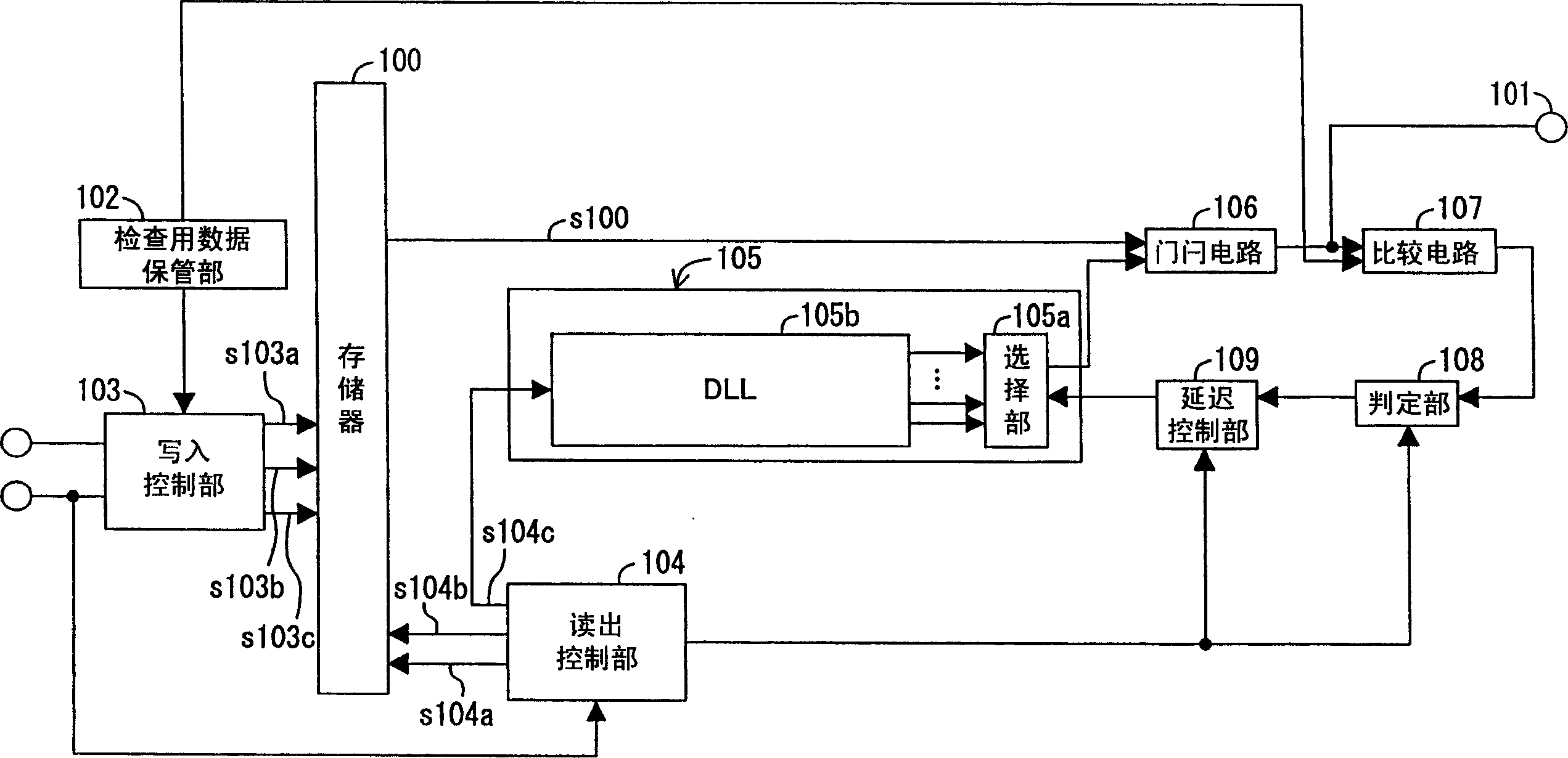
[0120] Next, a data latch timing adjustment device according to Embodiment 2 of the present invention will be described with reference to the drawings.

[0121] Figure 8 A data latch timing adjustment device according to Embodiment 2 of the present invention is shown. In this embodiment, the arrangement position of the delay selection unit 105 is changed.

[0122] that is in the figure 1 Among them, the delay selection unit 105 is arranged in the route for inputting the latch pulse signal from the readout control unit 104 to the gate latch circuit 106, and generates a plurality of delayed pulse signals. However, in this embodiment, the delay selection unit 105 The arrangement position of α is changed to the route for inputting the read data from the memory 100 to the latch circuit 106, and the read data is delayed by a plurality of delay amounts to generate a plurality of delayed output data. other structures with figure 1 Also, so its description is omitted.

[0123] Th...

Embodiment 3

[0134] Next, Embodiment 3 of the present invention will be described.

[0135] Figure 11 A data latch timing adjustment device according to Embodiment 3 of the present invention is shown. This embodiment shows an embodiment in which the memory 100 is composed of a DDR (Double Data Rate)-SDRAM that operates synchronously with both edges of a signal.

[0136] that is Figure 11In the middle, the memory 100 receives the clock signal CLK, and outputs data in synchronization with the rising edge and the falling edge of the clock signal CLK. Therefore, in this embodiment, two delay selectors 105A and 105B are provided, and the clock signal CLK is input as a latch pulse signal to one of the delay selectors 105A as it is, and the clock signal CLK is inverted. The inverter INV is inverted and input to the other delay selection unit 105B. Therefore, the one delay selection unit 105A is a latch for reading data at the rising edge of the clock signal CLK, and the other delay selectio...


PUM


Abstract

To automatically adjust latch timing for data, while reducing the number of latch circuits to be provided. A read controller 104 reads out first check data, which are written in a memory 100, from a check data storage part 102 and then outputs a latch pulse signal s104c to a delay selection part 105. The selection part 105a outputs a delayed pulse signal, with the latch pulse signal s104c being delayed at a leading delay circuit 1051, to a latch circuit 106. The latch circuit 106 latches the check data from the memory 100, when it receives the delayed pulse signal. Subsequently, next data is read out from the memory 100, and the selection part 105a outputs a delayed pulse signal, which is delayed at a delay circuit 1052 located in the following stage, to the latch circuit 106.

Description

technical field [0001] The present invention relates to a data latch timing adjustment device for adjusting the latch timing of data output from semiconductor circuits such as memories and LSIs. Background technique [0002] Generally, the timing of reading data from the memory is determined at the time of design, so the location or characteristics of the memory, the influence of ambient temperature, etc. will cause changes in the timing of data reading. If a fixed latch timing is used to latch the read data, a data latch error occurs. Therefore, it is necessary to adjust the latch timing of read data. In the past, in order to adjust the latch timing of the read data, a switch is provided to adjust the output data of the memory so that it can be latched normally. [0003] However, this method has a problem of steps to perform such an adjustment. For example, Patent Document 1 proposes a latch timing adjustment circuit that automatically adjusts the latch timing of data rea...

Claims


Application Information

Patent Timeline
Patent Type & Authority Applications(China)
IPC IPC(8): H03L7/081
CPCH03L7/0812H03L7/0816
Inventor 关口裕二三木阳一郎
Owner PANASONIC CORP
Why Eureka
Try Eureka