Flash memory cells and fabrication process thereof

A technology of flash memory unit and control gate, which is applied in semiconductor/solid-state device manufacturing, electrical components, information storage, etc.

Active Publication Date: 2004-06-30
SILICON STORAGE TECHNOLOGY
View PDF2 Cites 45 Cited by
  • Summary
  • Abstract
  • Description
  • Claims
  • Application Information

AI Technical Summary

Problems solved by technology

[0007] Using 3P self-aligned split gate cell structure and unique programming and erasing technology, although the cell size can be made smaller than the size of the commonly used ETOX structure, but as the cell

Method used


Image

  • Flash memory cells and fabrication process thereof
  • Flash memory cells and fabrication process thereof
  • Flash memory cells and fabrication process thereof

Examples


Embodiment Construction

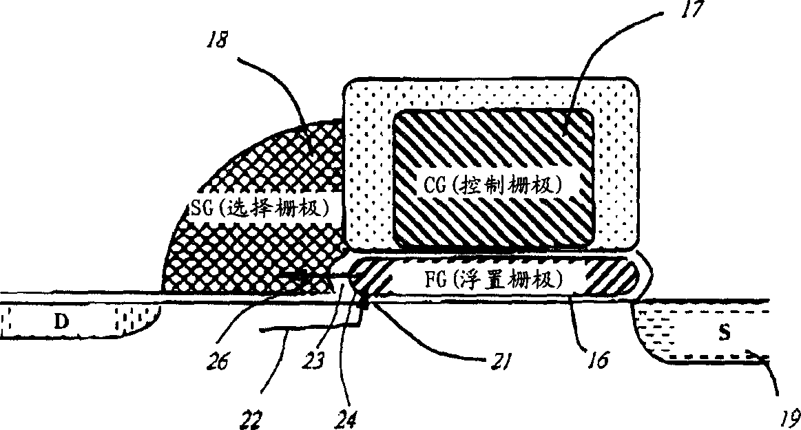
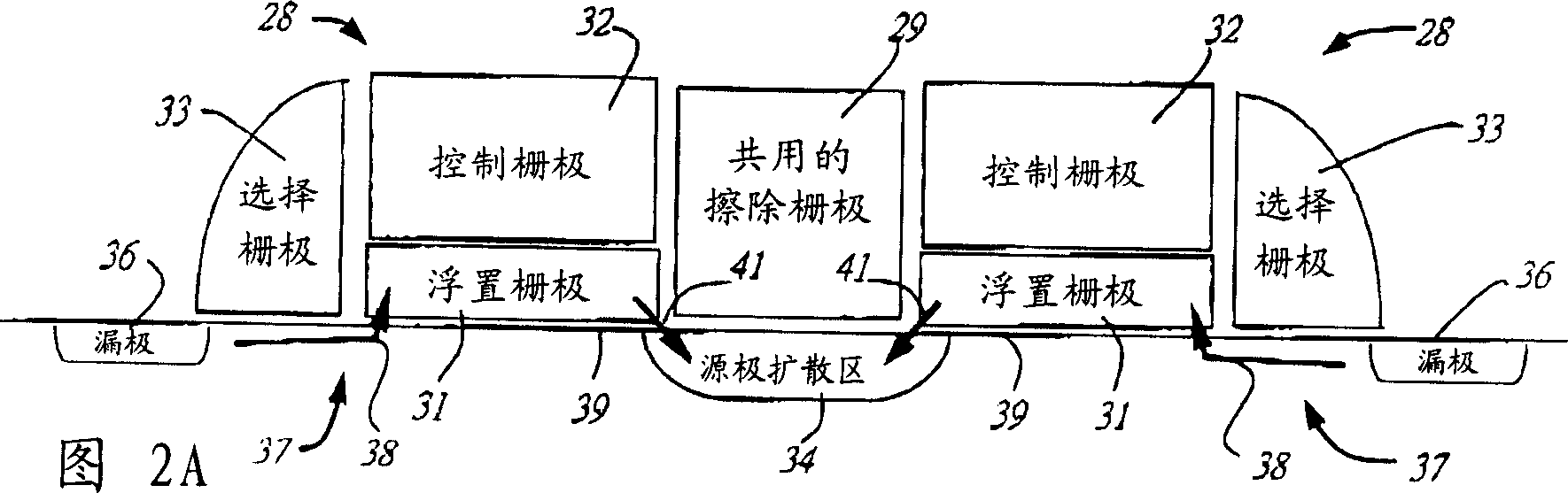
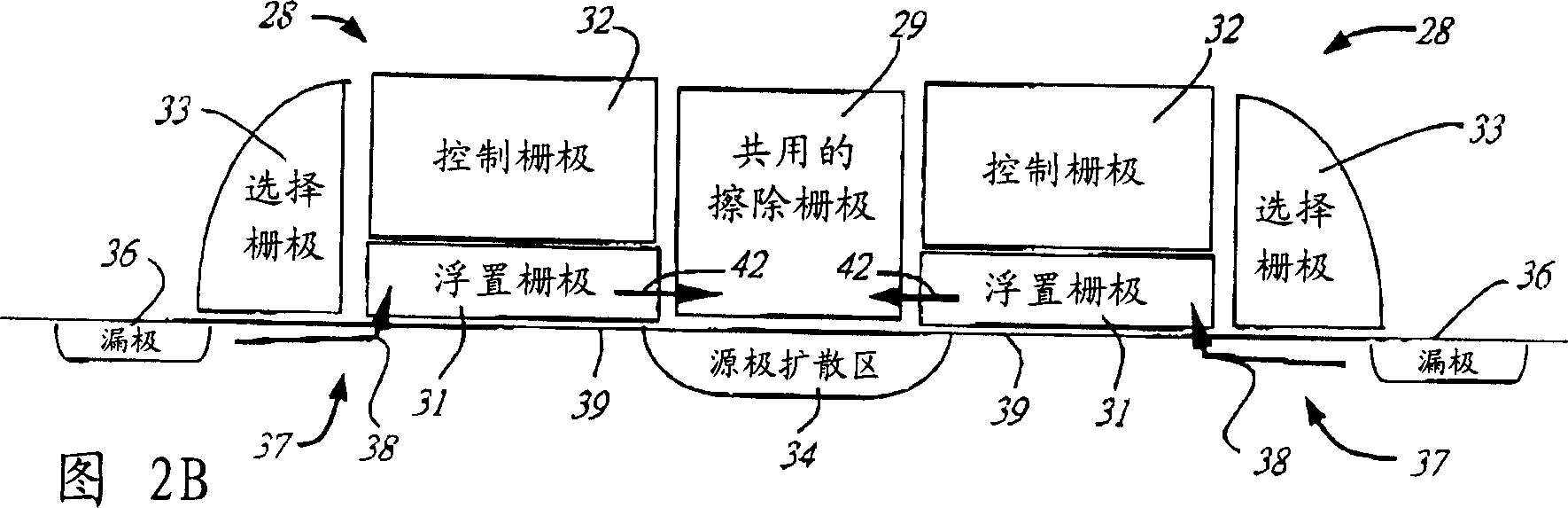
[0021] In the embodiment of FIGS. 2A and 2B , two memory cells 28 share a common erase gate 29 . Each cell has a vertically stacked self-aligned floating gate 31 and a control gate 32, the floating gate 31 is relatively thin (eg, 100 Å to 700 Å) and the control gate 32 is located above the floating gate . Each cell also has a select gate 33 on one side of the stacked floating and control gates. The select and erase gates are formed simultaneously from a polysilicon layer deposited across the entire wafer and then etched anisotropically in a dry etching process.

[0022] Source and drain diffusion regions 34 and 36 are formed in the substrate, the source regions extending under edge portions of the erase gate and the floating gate. The drain region extends under an edge portion of the select gate opposite the stacked gate and is shared with a select gate in an adjacent cell (not shown).

[0023] In these embodiments, programming occurs in the central channel region 37 betwee...


PUM


Abstract

Vertical contraposed pair of floating grid and control grid is formed at side opposite to source diffusion zone in substrate. Erasing grid is formed between above source diffusion zone and contraposed grid. Selecting grid is formed is formed at side opposite to contraposed grid and erasing grid. Programming channel is extended from intermediate channel region on substrate to peripheral part of the selecting grid faced to the floating grid. Erasing channel is extended from peripheral part of the erasing grid faced to the floating grid to the source diffusion zone and the erasing grid. In some instances, the source diffusion zone is connected to the erasing grid electrically. In other instances, the floating grid stands out one or two sides of the control grid laterally. Comparing with prior art, the invention provides better programming and erasing performances with very small size of storage cell.

Description

technical field [0001] The present invention relates generally to semiconductor memory devices, and more particularly to nonvolatile memories and methods of manufacturing the same. Background technique [0002] There are several forms of non-volatile memory currently available, including electrically programmable read-only memory (EPROM), electrically erasable programmable read-only memory (EEPROM), and flash EEPROM. [0003] US Patents 6,091,104 and 6,291,297 disclose a split gate memory cell with relatively small size, efficient erase performance and relatively small programming current requirements. The small size is achieved by the self-alignment of the select gate, control gate and floating gate, and by utilizing the Fowler-Nordheim tunneling from the sharply curved sides of the floating gate to the select gate Tunneling (Fowler-Nordheim tunneling) provides erasing efficiency. The programming current is kept small by utilizing center channel hot carrier injection from...

Claims


Application Information

Patent Timeline
IPC IPC(8): H01L21/8247H01L27/115H01L29/423
CPCH01L27/11521H01L29/42328H01L27/115G11C16/0425H01L29/7883H10B41/30
Inventor 范德慈陈秋峰普拉蒂普·滕塔苏德
Owner SILICON STORAGE TECHNOLOGY
Why Eureka
Try Eureka