Field-emisson displaing device with grid board

A display and field emission technology, applied in the direction of static indicators, cathode ray/electron beam tube casing/container, image/graphic display tube, etc. Wear phenomenon, improve production efficiency and output effect

Inactive Publication Date: 2004-07-07
ELECTRONICS & TELECOMM RES INST
View PDF0 Cites 13 Cited by
  • Summary
  • Abstract
  • Description
  • Claims
  • Application Information

AI Technical Summary

Problems solved by technology

[0017] Therefore, the conventional active matrix field emission display has the disadvantage that the voltage applied to the anode electrode 24 is limited by the breakdown characteristics of the control device 23, and it is difficult to manufacture a field emission display with high brightness due to the limitation of the anode voltage.

Method used


Image

  • Field-emisson displaing device with grid board
  • Field-emisson displaing device with grid board
  • Field-emisson displaing device with grid board

Examples


Embodiment Construction

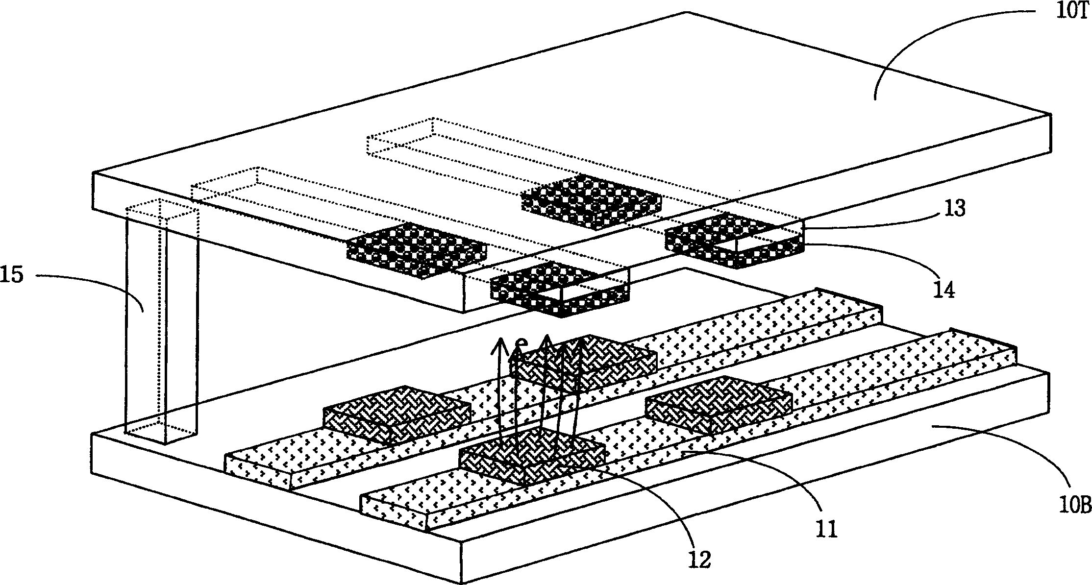
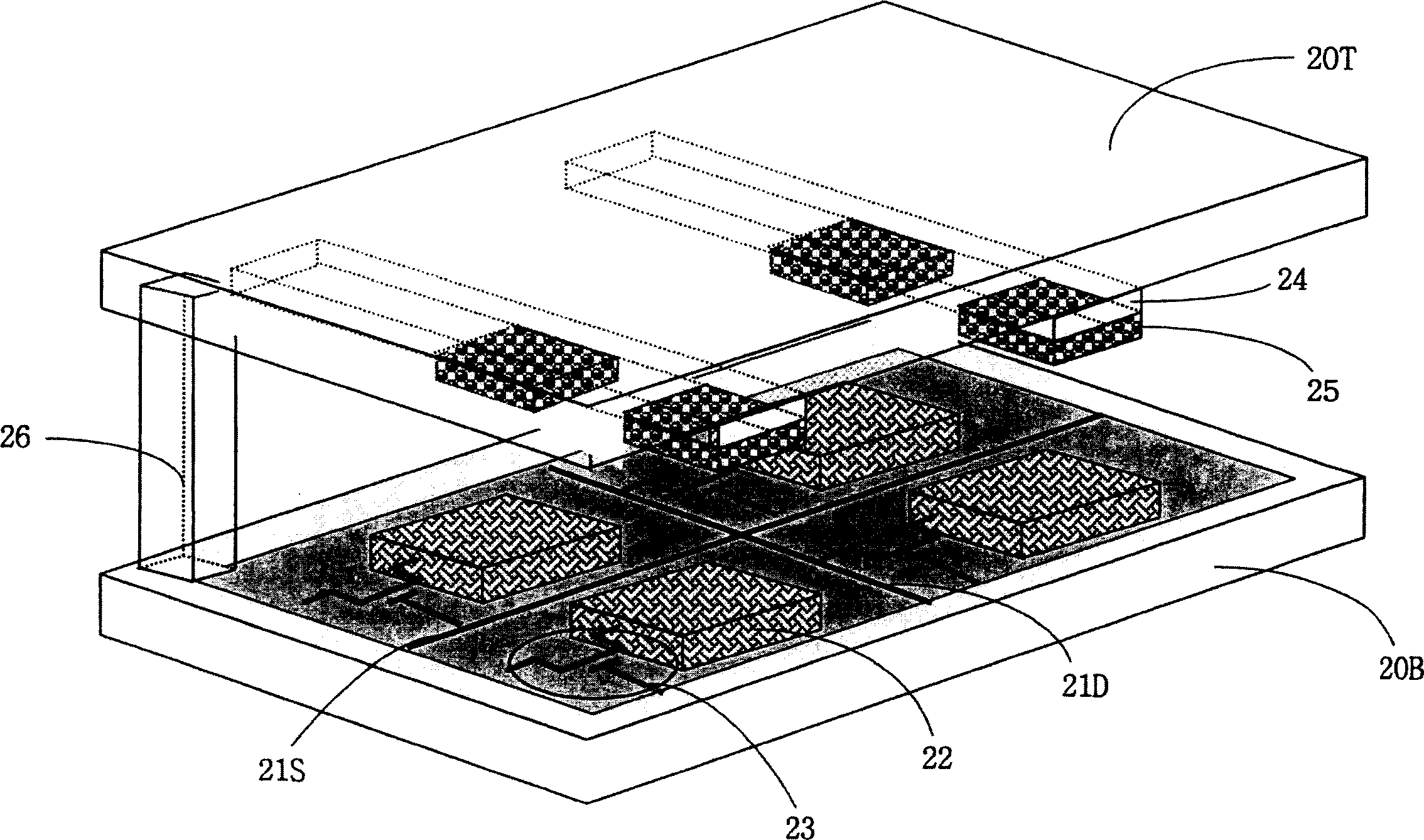
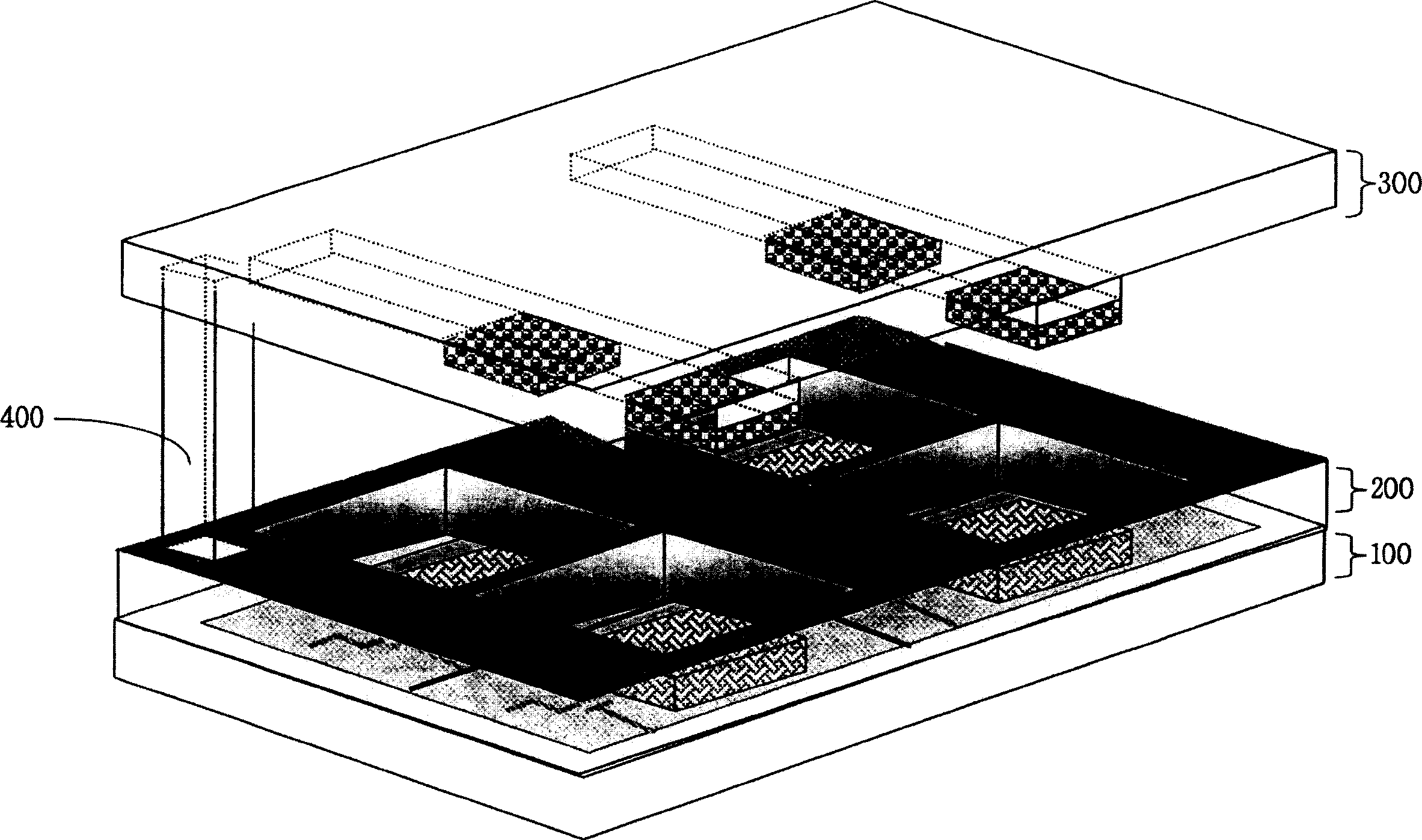
[0042] Compared with the field emission display in the prior art, the field emission display of the present invention has significant differences in the structure of the cathode plate and the grid plate and their driving methods. Below, will refer to Figure 3 to Figure 8 The field emission display according to the present invention will be described in detail.

[0043] image 3 is a perspective view concisely showing the structure of an active matrix field emission display with a grid plate according to the present invention, Figure 4 is a perspective view concisely showing a cathode plate, a grid plate and an anode plate in the field emission display according to the present invention. The field emission display includes a cathode plate 100 , a grid plate 200 and an anode plate 300 .

[0044] Such as Figure 4 As shown, the cathode plate 100 includes strip-shaped row signal lines 120S and column signal lines 120D on an insulating substrate 110 containing glass, plastic,...


PUM


Abstract

The present invention relates to a field emission display in which a gate plate having a gate hole and a gate electrode around the gate hole is formed between an anode plate having phosphor and a cathode plate having a field emitter and a control device for controlling field emission current, wherein the field emitter of the cathode plate is constructed to be opposite to the phosphor of the anode plate through the gate hole. According to the present invention, it is possible to significantly reduce the display row / column driving voltage by applying scan and data signals of the field emission display to the control device of each pixel, And the present invention is directed to improve the brightness of the field emission display in such a manner that the electric field necessary for field emission is applied through the gate electrode of the gate plate to freely control the distance between the anode plate and the cathode plate, so that a high voltage can be applied to the anode.

Description

technical field [0001] The present invention relates to a kind of field emission display (FED) that field emission device is applied to flat panel display, relate in particular to a kind of field emission display, wherein have field emitter and be used to control field emission current in an anode plate with phosphor A grid plate is formed between a cathode plate of the control device, and the grid plate has a grid hole and a grid electrode around the grid hole, wherein the field emitter of the cathode plate passes through the grid hole and the grid electrode of the anode plate Phosphor relative configuration. Background technique [0002] A field emission display is a device that displays images through the cathode electron excitation light of a phosphor, using electrons emitted from the field emitter of the cathode plate to collide with the phosphor of the anode plate, where the cathode plate with the field emitter and the phosphor with the phosphor The anode plates are o...

Claims


Application Information

Patent Timeline
Patent Type & Authority Applications(China)
IPC IPC(8): H01J29/04G09G3/20G09G3/22H01J1/62H01J29/02H01J29/32H01J29/46H01J29/48H01J29/87H01J29/96H01J31/12H01J63/04
CPCH01J29/467H01J31/127H01J29/028H01J2329/8625H01J29/481
Inventor 宋润镐黄治善李镇浩郑重熙
Owner ELECTRONICS & TELECOMM RES INST
Why Eureka
Try Eureka