Filed-effect tube channel type field emission cathode and preparation method thereof

A tube-channel type, field emission technology, applied in cold cathode manufacturing, electrode system manufacturing, discharge tube/lamp manufacturing, etc., can solve the problem of difficult control of stability, and achieve the effect of uniform and stable field emission current

Inactive Publication Date: 2015-10-21
XI AN JIAOTONG UNIV
View PDF5 Cites 4 Cited by
  • Summary
  • Abstract
  • Description
  • Claims
  • Application Information

AI Technical Summary

Problems solved by technology

Due to the exponential dependence of the emission current and the external field strength, the stability is difficult to control; secondly, because the three-dimensional grid structure is a capacitive structure, this will limit the upper limit of its modulation frequency

Method used


Image

  • Filed-effect tube channel type field emission cathode and preparation method thereof
  • Filed-effect tube channel type field emission cathode and preparation method thereof
  • Filed-effect tube channel type field emission cathode and preparation method thereof

Examples


example 1

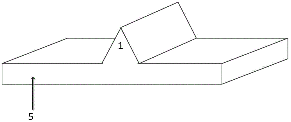
[0027] 1) A one-dimensional nano-edge is etched on the substrate. This solution uses Si-SiO 2 as a substrate. Firstly, in highly doped Si-SiO 2 A 2um-wide strip mask pattern is photo-etched on the wafer, and the SiO unprotected by the photoresist is etched using an HF etching solution. 2 layer, and the SiO was observed under the microscope 2 Come off to stop. Then, a KOH anisotropic etching solution obtained by mixing 1 mol / L isopropanol (IPA) and 5 mol / L KOH was used to etch to fabricate Si wedges. The temperature of the etching solution is 60° C. to 63° C., and the etching time is 6 to 7 minutes. Do not stir the corrosion solution during the corrosion process. A certain proportion of isopropanol can increase the corrosion rate ratio of different crystal planes R(111) / (100). The corrosion container should be relatively airtight, and isopropanol should also be added to the water bath to maintain The stability of the ratio of isopropanol in the corrosion solution. Finall...

example 2

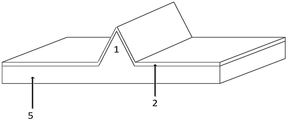
[0033] 1) Fabrication and etching of the metal mask layer on the substrate. First, a layer of 10nm thick metal Cr is magnetron sputtered on the Si substrate, and then a photoresist mask pattern with a width of 2um is produced on the metal Cr by a photolithography process. Dry the sample and place it in the prepared solution of corroding metal Cr, the solution is ammonium cerium nitrate (H 4 CeN 2 o 3 ): Glacial acetic acid (C 2 h 4 o 2 ): deionized water=10g: 2.5mL: 50g, after about 3 minutes, the patterned Cr mask layer can be seen.

[0034] Then, the substrate is subjected to alternate compound deep etching by ICP, and the etching gas and passivation gas are respectively SF 6 and C 4 f 8 . Place the silicon wafer sample protected by the Cr mask layer in the reaction chamber, and after the pressure in the chamber is pumped to 2-3Pa by the mechanical pump, continue to vacuum to 3.0×10 -3 Pa, respectively circulating the reaction gas SF 6 and C 4 f 8 , the flow rat...

example 3

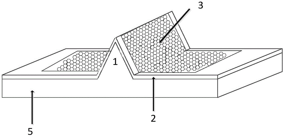
[0039] 1)Al 2 o 3 of etching. Using photoresist AZ4620 on Al 2 o 3 A strip mask pattern with a width of 4um and a height of 4um is fabricated on the substrate, and then ICP etching is performed. Two steps are used for etching: in the first step, the ICP power and bias power are set to 1475W and 290W respectively, the chamber tray temperature is 25°C, BCl 3 Gas flow rate is 85cm 3 / min; In the second step, increase the bias power to 450W. At this time, the photoresist has been completely etched. Through a high bias power, the sapphire substrate is etched quickly, making the edge of the cone more straight .

[0040] 2) CVD in-situ growth of graphene. In edged Al 2 o 3 A layer of 200nm thick metallic Ni was deposited on the substrate as a catalyst. The growth temperature is 1000°C, the heating rate is 0.5°C / s, the growth time is 1h, CH 4 with H 2 The flow ratio is 10sccm: 40sccm.

[0041] After the growth is finished, place the sample in 0.5mol / L FeCl3 solution for e...


PUM


Abstract

The invention discloses a field-effect tube channel type field emission cathode and a preparation method thereof. The cathode is modulated by a back gate and drain voltage. Additional bias voltage is used for changing electronic supply functions in two dimensional materials used as conductive channels, thereby adjusting field emission current density and achieving a field emission cold cathode modulated by the electric field. A new solution is provided for improving stability of field emission current of two-dimensional nano-materials, and a new path is provided for achievement of high-frequency regulated field emission cathode, thereby promoting actual application of two-dimensional nano cold cathodes with low emission threshold voltage in the vacuum microelectronic field.

Description

technical field [0001] The invention belongs to the field of vacuum microelectronics, and relates to a field emission cathode modulated by an external channel bias voltage and a back grid voltage and a preparation method thereof. Background technique [0002] Integrated vacuum electronic devices require the cathode to have higher electron beam current density output, higher operating frequency, smaller cathode size and higher assembly precision. Compared with hot cathodes, which rely on increasing the kinetic energy of electrons to escape the surface barrier of materials, field emission cathodes with higher emission efficiency are the most promising solutions for integrated vacuum electronics. The development of field emission cathodes has gone through the earliest Spindt-type cathodes to nano-cold cathodes in recent years. The practical application of Spindt-type cathode technology is not smooth. Taking the silicon cone field emission array as an example, even thanks to th...

Claims


Application Information

Patent Timeline
Patent Type & Authority Applications(China)
IPC IPC(8): H01J1/312H01J9/02
Inventor 刘卫华王小力曹桂铭李昕曹猛
Owner XI AN JIAOTONG UNIV
Why Eureka
Try Eureka