Isolated gate controlled transverse field emission transistor and driving method thereof

A driving method and lateral field technology, applied in semiconductor devices, semiconductor/solid-state device manufacturing, electrical components, etc., can solve problems such as the influence of carrier mobility and current density, and the small channel length of MOS field effect transistors.

Inactive Publication Date: 2013-01-02
INST OF MICROELECTRONICS CHINESE ACAD OF SCI
View PDF5 Cites 4 Cited by
  • Summary
  • Abstract
  • Description
  • Claims
  • Application Information

AI Technical Summary

Problems solved by technology

[0003] However, with the further reduction of the device size, the channel length of the MOS field effect transistor becomes very small, and the ejection movement of the carriers in the short-distance

Method used


Image

  • Isolated gate controlled transverse field emission transistor and driving method thereof
  • Isolated gate controlled transverse field emission transistor and driving method thereof
  • Isolated gate controlled transverse field emission transistor and driving method thereof

Examples


Embodiment Construction

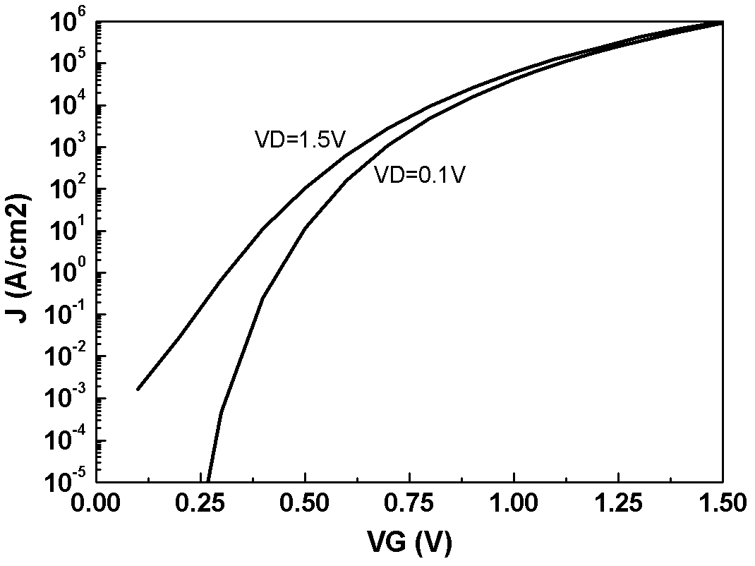
[0038] The performance of conventional MOS field effect transistors in the prior art is limited by the transport characteristics of carriers in the crystal lattice of the channel region, and it is difficult to meet the requirements of continuous development of the process.

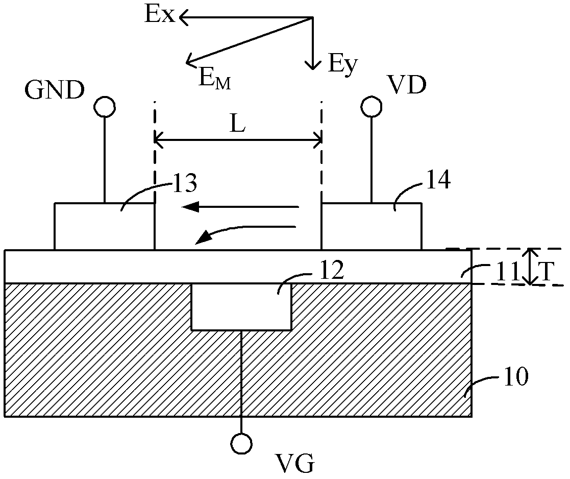
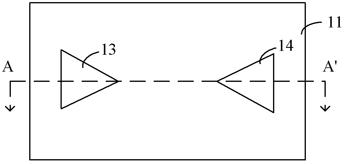
[0039] An embodiment of the present invention provides an insulated gate-controlled lateral field emission transistor, comprising a first gate dielectric layer, a first gate electrode, a collector and an emitter, wherein the first gate electrode is located on the first surface of the first gate dielectric layer The collector and the emitter are located on the second surface of the first gate dielectric layer, on both sides of the first gate electrode, and the collector and the emitter are insulated from each other with a gap between them. When driving it, a driving voltage is applied between the collector and the emitter, so that the emitter emits electrons to the collector to generate a field emission curr...


PUM

PropertyMeasurementUnit
Thicknessaaaaaaaaaa

Abstract

The invention relates to an isolated gate controlled transverse field emission transistor and a driving method thereof. The transistor comprises a first gate dielectric layer, a first gate electrode, a collector electrode and an emitter electrode, wherein the first gate dielectric layer is provided with a first surface and a second surface which are opposite to each other; the first gate electrode is arranged on a first surface of the first gate dielectric layer; the collector electrode and the emitter electrode are arranged on a second surface of the first gate dielectric layer and at both sides of the first gate electrode; and the collector electrode and the emitter electrode are insulated from each other, and a gas is formed between the collector electrode and the emitter electrode. According to the invention, electric conduction is realized through a field emission current from the emitter electrode to the collector electrode in the field effect transistor, and a current switch of transverse field emission from the emitter electrode to the collector electrode is controlled by the first gate electrode at the same time, so that limitation in carrier transport by a lattice structure of a channel region in a conventional MOS ( field effect transistor) is eliminated, the need of process development can be met, and the transistor has a higher response speed.

Description

technical field [0001] The invention relates to the field of semiconductor devices, in particular to an insulated gate-controlled lateral field emission transistor and a driving method thereof. Background technique [0002] With the development of semiconductor technology and the continuous reduction of critical dimensions (CD, Critical Dimension), the challenges faced by conventional MOS field effect transistors are becoming more and more severe. For conventional MOS field effect transistors, the movement modes of carriers in the channel mainly include drift, diffusion and scattering. In order to improve carrier mobility, the current mainstream technology is strained silicon technology, which mainly introduces stress, such as tensile stress or compressive stress, to the channel region of MOS transistors, thereby changing the lattice structure of the channel region and improving the current carrying capacity. sub-transport efficiency. [0003] However, with the further red...

Claims


Application Information

Patent Timeline
IPC IPC(8): H01L29/417H01L29/76H01L21/334
Inventor 殷华湘董立军陈大鹏
Owner INST OF MICROELECTRONICS CHINESE ACAD OF SCI
Why Eureka
Try Eureka