LCD device and its electronic device
一种液晶显示装置、液晶的技术,应用在机械设备、管子、管子/管接头/管件等方向,能够解决影响大、液晶倾倒、透射率降低等问题
- Summary
- Abstract
- Description
- Claims
- Application Information
AI Technical Summary
Problems solved by technology
Method used
Image

Examples
no. 1 Embodiment approach
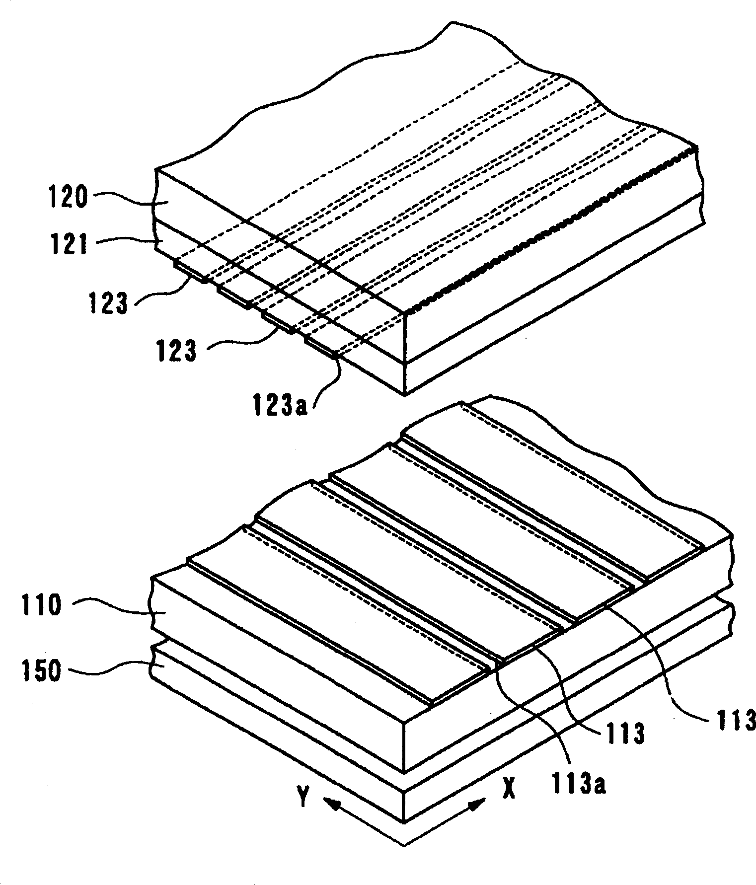
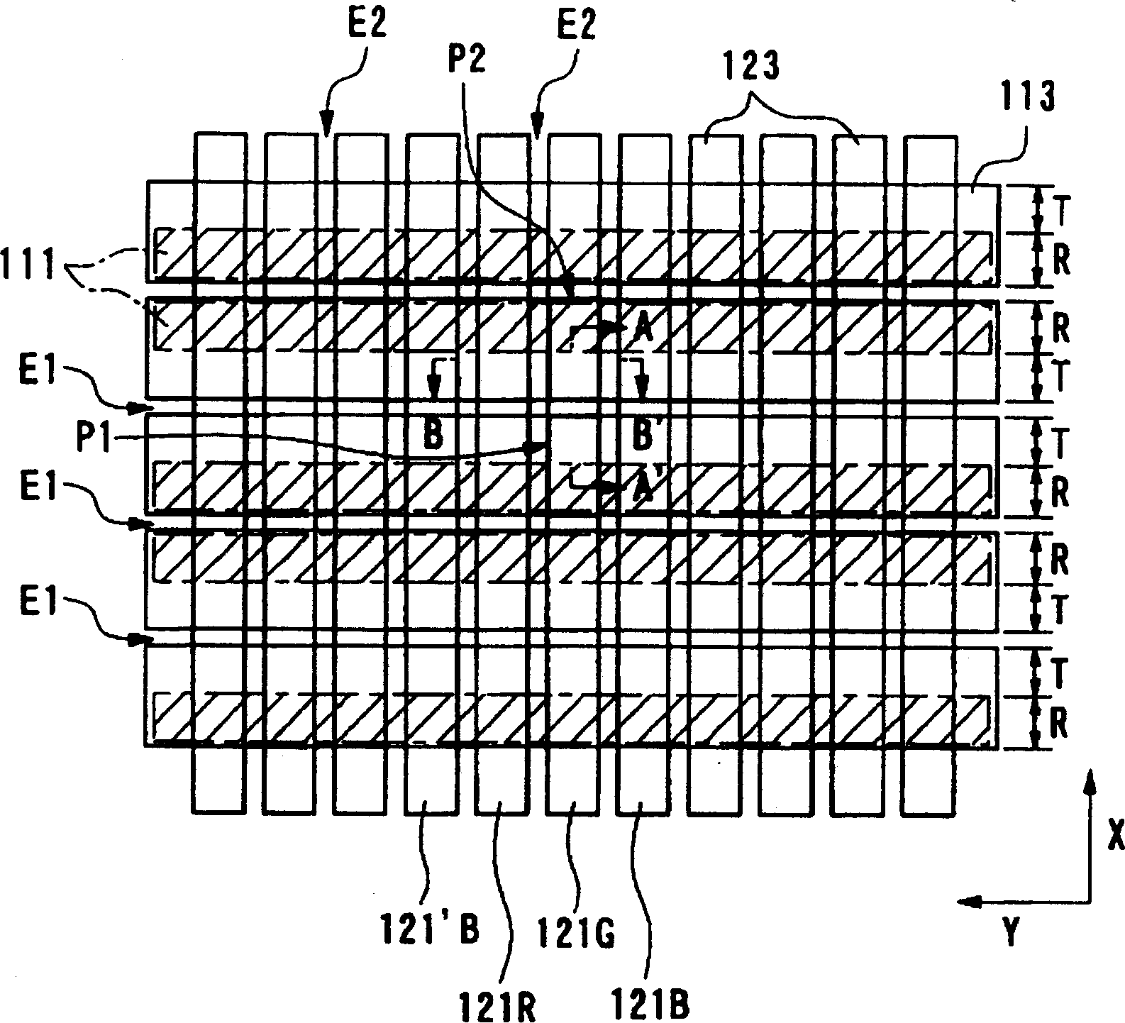
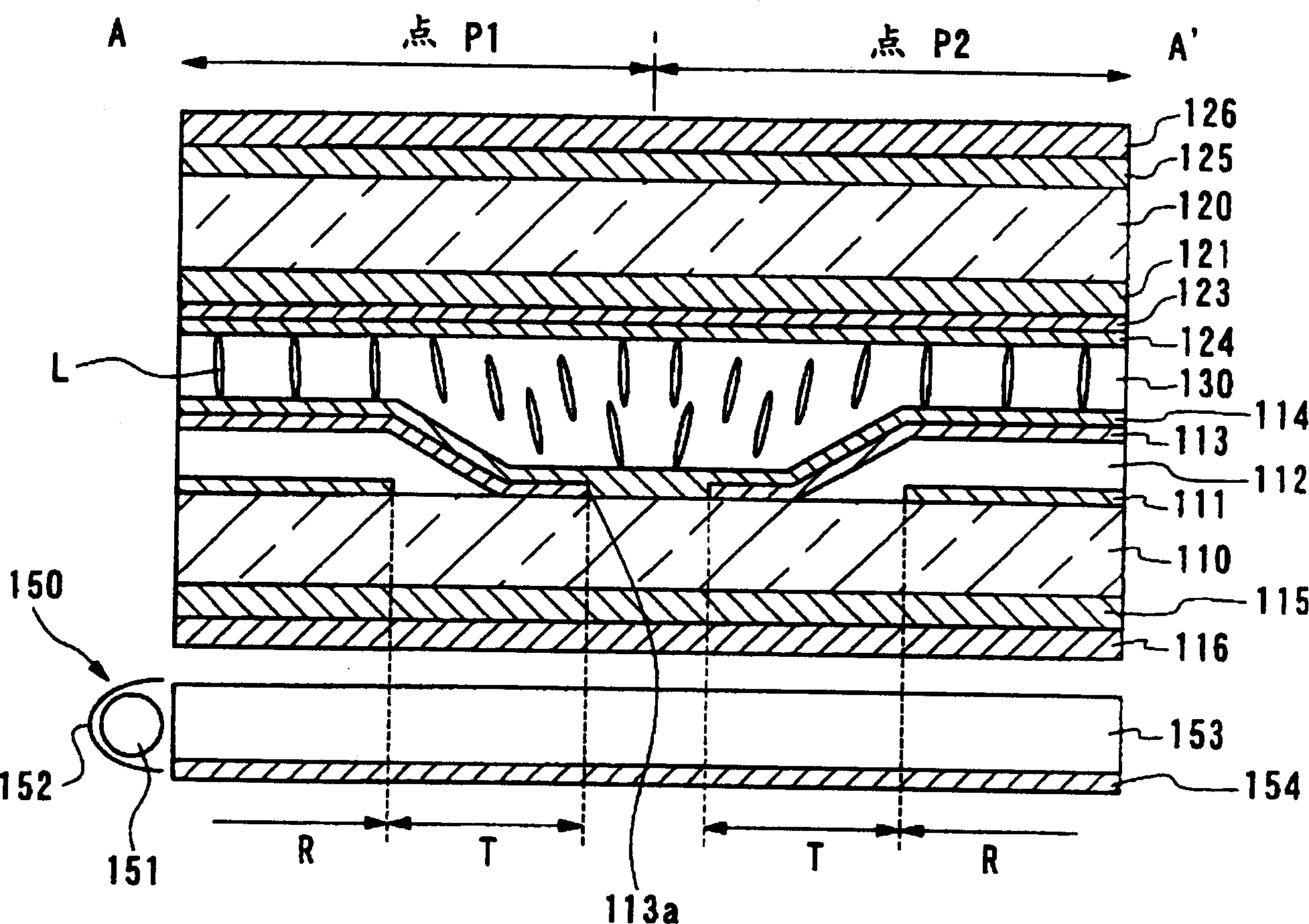
[0050] Refer below Figure 1-Figure 5 A liquid crystal display device according to a first embodiment of the present invention will be described. figure 1 is a perspective view showing a schematic configuration of a liquid crystal display device according to this embodiment, figure 2 is a plan view showing its principal parts, image 3 is a cross-sectional view of its main parts, Figure 4 is a cross-sectional diagram illustrating its function, Figure 5 It is a plan view showing the alignment state of liquid crystal molecules. In addition, in each of the following figures, in order to make each layer or each component recognizable on the drawing, the scaling ratios of the respective dimensions of each layer or each component are different. In addition, in this specification, the surface arrange|positioned by the liquid crystal layer side among each member which comprises a liquid crystal device is called "inner surface", and the surface on the opposite side is called "ou...
no. 2 Embodiment approach
[0091] Next, refer to Figure 8-Figure 10 A liquid crystal display device according to a second embodiment of the present invention will be described. Figure 8 is a perspective view showing a schematic configuration of a liquid crystal display device according to this embodiment, Figure 9 is a cross-sectional view of its main parts, Figure 10 It is a plan view showing the alignment state of liquid crystal molecules.
[0092] First, based on Figure 8 The schematic structure of the liquid crystal display device of this embodiment is demonstrated.
[0093] The liquid crystal display device of the present embodiment is an active matrix liquid crystal display device, and a substantially rectangular pixel electrode 213 is formed on the lower substrate 210 as a TFT array substrate, and a common electrode 223 is formed on the upper substrate 220 of the opposite substrate. . A plurality of pixel electrodes 213 are arranged in a matrix on the lower substrate 210 , and the regio...
PUM
| Property | Measurement | Unit |
|---|---|---|
| coating thickness | aaaaa | aaaaa |
Abstract
Description
Claims
Application Information
 - R&D
- Intellectual Property
- Life Sciences
- Materials
- Tech Scout
- Unparalleled Data Quality
- Higher Quality Content
- 60% Fewer Hallucinations
Browse by: Latest US Patents, China's latest patents, Technical Efficacy Thesaurus, Application Domain, Technology Topic, Popular Technical Reports.
© 2025 PatSnap. All rights reserved.Legal|Privacy policy|Modern Slavery Act Transparency Statement|Sitemap|About US| Contact US: help@patsnap.com