Structure for addressing electrodes in plasma panel display
A flat-panel display and addressing electrode technology, applied to cold cathode tubes, solid cathode components, etc., can solve the problems of slow writing speed, high probability of disconnection, and low current, so as to increase writing speed and improve current resistance ability to avoid the effect of overloading
- Summary
- Abstract
- Description
- Claims
- Application Information
AI Technical Summary
Problems solved by technology
Method used
Image
Examples
Embodiment Construction
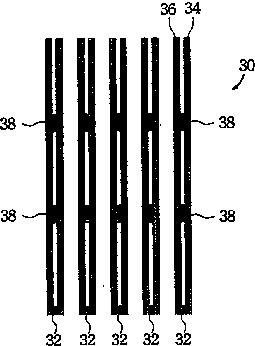
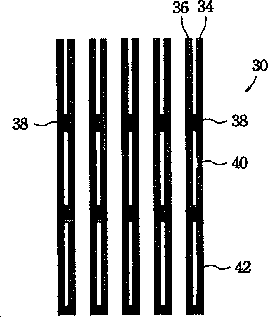
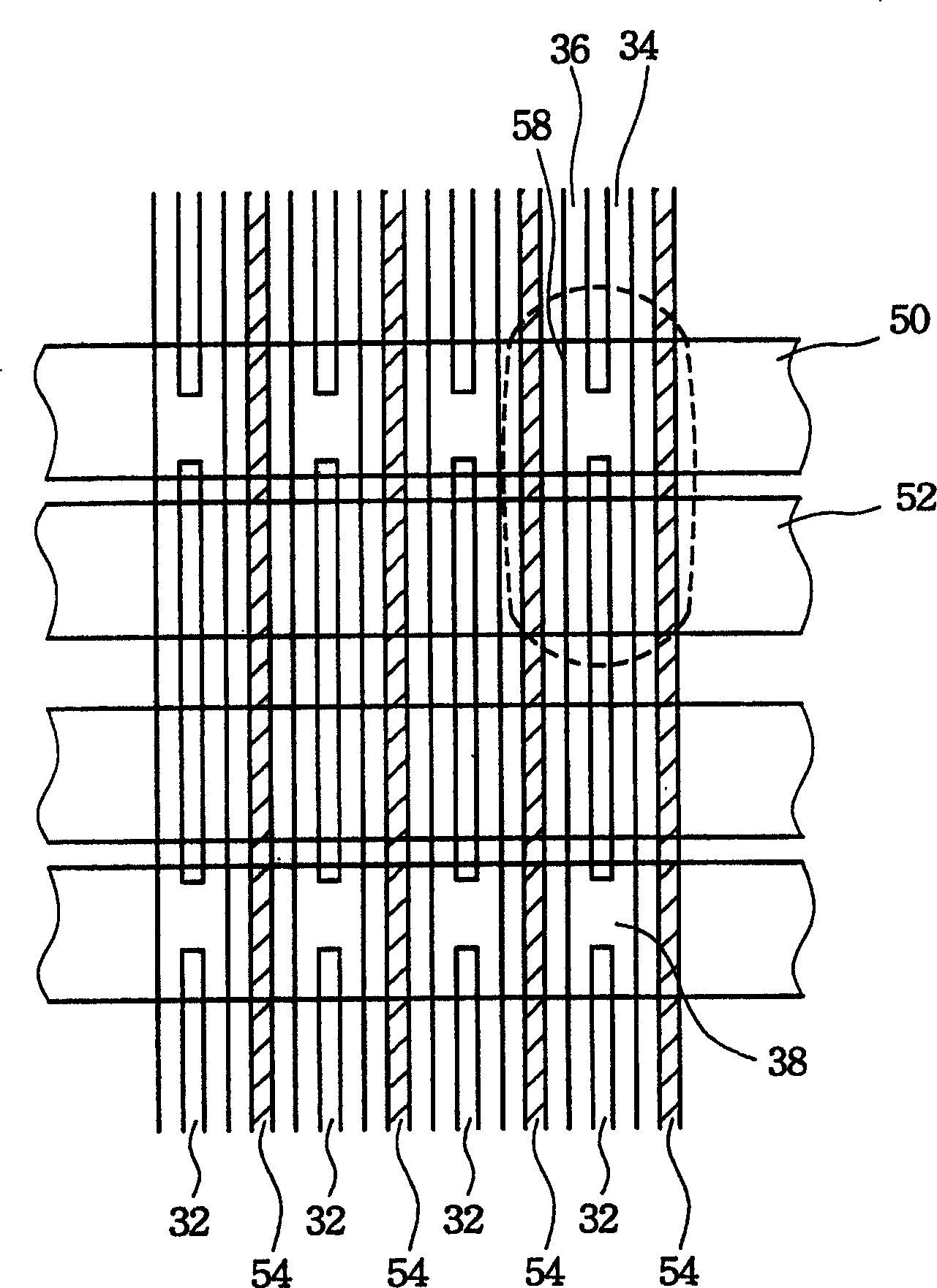
[0029] Without limiting the spirit and scope of application of the present invention, the implementation of the present invention is described below with an embodiment; those of ordinary skill in the art, after understanding the spirit of the present invention, can apply the addressing electrode of the present invention structure in various plasma displays. Each addressing electrode structure is composed of two wires, which are connected at the adjoining positions of the X electrode and the Y electrode close to the light-emitting unit, thereby increasing the writing speed. The application of the present invention should not be limited to the preferred embodiments described below.
[0030] Such as figure 1 Shown is a schematic top view of the address electrode structure of a plasma flat panel display according to a preferred embodiment of the present invention. The addressing electrode structure 30 of the present invention adopts the design of two wires, that is, each address...
PUM
 Abstract
Description
Claims
Application Information


