Low-thickness current-withstanding SiC PIN diode and manufacturing method thereof

A current-resistant, low-thickness technology, used in semiconductor/solid-state device manufacturing, circuits, electrical components, etc., to solve problems such as limited improvement

Pending Publication Date: 2022-01-21
GLOBAL POWER TECH CO LTD
View PDF0 Cites 0 Cited by
  • Summary
  • Abstract
  • Description
  • Claims
  • Application Information

AI Technical Summary

Problems solved by technology

[0003] However, limited by material characteristics, the intrinsic breakdown field strength is determined. The main way to improve the withstand voltage of PIN diodes is to improve the terminal structure, and to obtain higher withstand voltage PIN diodes by optimizing the doping method, so the degree of improvement is very limited.

Method used


Image

  • Low-thickness current-withstanding SiC PIN diode and manufacturing method thereof
  • Low-thickness current-withstanding SiC PIN diode and manufacturing method thereof
  • Low-thickness current-withstanding SiC PIN diode and manufacturing method thereof

Examples


Embodiment Construction

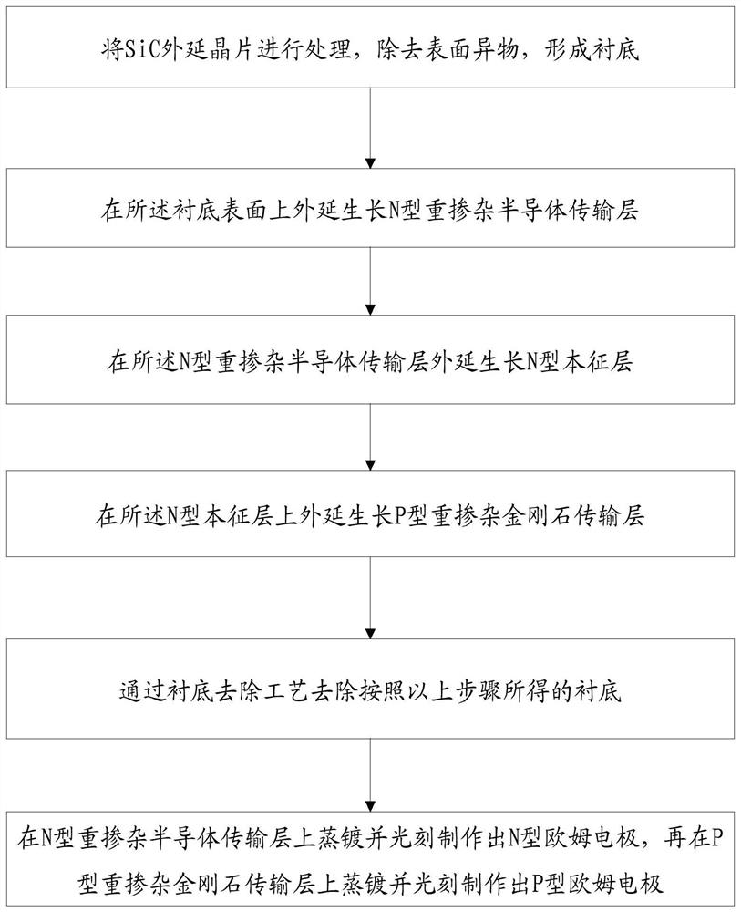
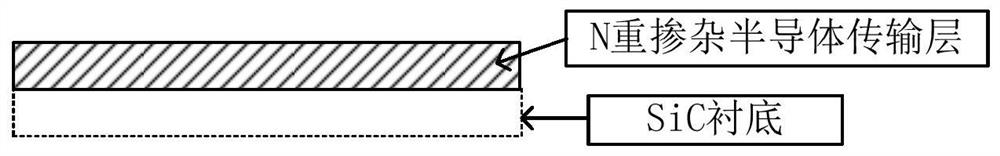
[0035] Such as Figure 1 to Figure 7 As shown, a method for manufacturing a low-thickness current-resistant SiC PIN diode of the present invention includes:

[0036] Step 1. Rinse the surface of the SiC epitaxial wafer with deionized water, and then soak it in a heated mixed washing solution for 1 minute to further remove foreign matter on the surface of the SiC epitaxial wafer to form a substrate; the mixed washing solution includes ammonia water, hydrogen peroxide, and deionized Ionized water;

[0037] Step 2, epitaxially growing an N-type heavily doped semiconductor transport layer on the surface of the substrate;

[0038] Step 3, epitaxially growing an N-type intrinsic layer on the N-type heavily doped semiconductor transport layer;

[0039] Step 4. Epitaxially grow a P-type heavily doped diamond transport layer on the N-type intrinsic layer, and the doping concentration of the P-type heavily doped diamond transport layer is 2*10 19 cm -3 , the thickness of the P-type ...


PUM

PropertyMeasurementUnit
thicknessaaaaaaaaaa

Abstract

The invention provides a low-thickness current-resistant SiC PIN diode and a manufacturing method thereof. The diode is characterized in that the lower side surface of an N-type heavily-doped semiconductor transmission layer is connected to the upper side surface of an N-type ohmic electrode; the lower side surface of an N-type intrinsic layer is connected to the upper side surface of the N-type heavily-doped semiconductor transmission layer; the lower side surface of a P-type heavily-doped diamond transmission layer is connected to the upper side surface of the N-type intrinsic layer; and the lower side surface of a P-type ohmic electrode is connected to the upper side surface of a P-type heavily-doped diamond transmission layer. Thus, the thickness of the diode is reduced, and current-withstanding capability is increased by four times.

Description

technical field [0001] The invention relates to a low-thickness current-resistant SiC PIN diode and a manufacturing method thereof. Background technique [0002] SiC device Silicon carbide (SiC) material has been widely concerned and researched due to its superior physical properties. Its high-temperature and high-power electronic devices have the advantages of high input impedance, fast switching speed, high operating frequency, high temperature and high pressure resistance, etc., and have been widely used in switching regulated power supplies, high-frequency heating, automotive electronics, and power amplifiers. [0003] However, limited by material characteristics, the intrinsic breakdown field strength is determined. The main way to improve the withstand voltage of PIN diodes is to improve the terminal structure, and to obtain higher withstand voltage PIN diodes by optimizing the doping method, so the degree of improvement is very limited. . Contents of the invention ...

Claims


Application Information

Patent Timeline
Patent Type & Authority Applications(China)
IPC IPC(8): H01L29/06H01L29/16H01L29/868H01L21/329
CPCH01L29/0684H01L29/1608H01L29/868H01L29/6606
Inventor 张瑜洁施广彦李佳帅李志君黄波
Owner GLOBAL POWER TECH CO LTD
Why Eureka
Try Eureka