

Method of manufacturing semiconductor device
A manufacturing method and semiconductor technology, which can be used in the manufacture of semiconductor/solid-state devices, semiconductor devices, transistors, etc., and can solve problems such as aggravating the increase of defect rate and the decrease of reliability.
- Summary
- Abstract
- Description
- Claims
- Application Information
AI Technical Summary
Problems solved by technology
Method used
Image

Examples
Embodiment Construction
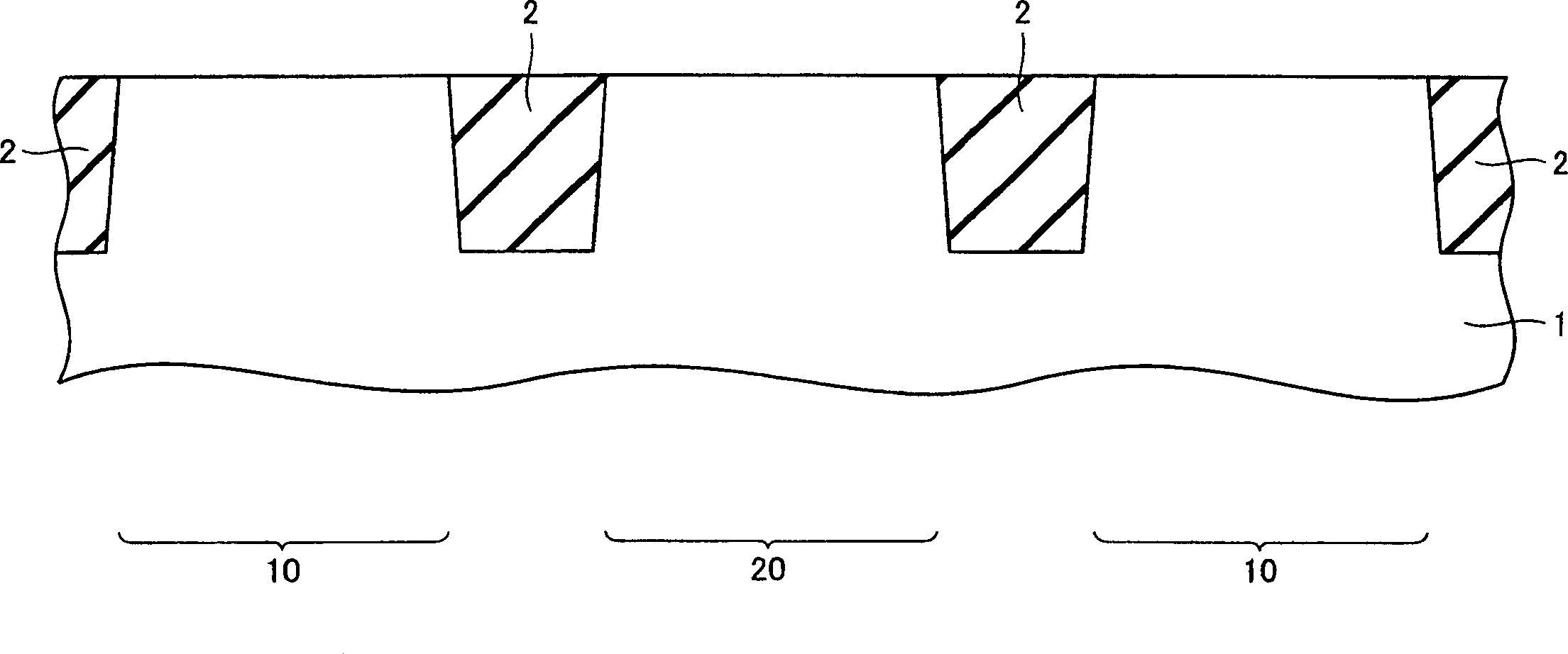
[0020] The method of manufacturing a semiconductor device in an embodiment of the present invention will be described in detail with reference to the drawings and divided into individual steps. Furthermore, the semiconductor device manufacturing method in the embodiment of the present invention is an example of forming field effect transistors in an array on the main surface of a semiconductor substrate.
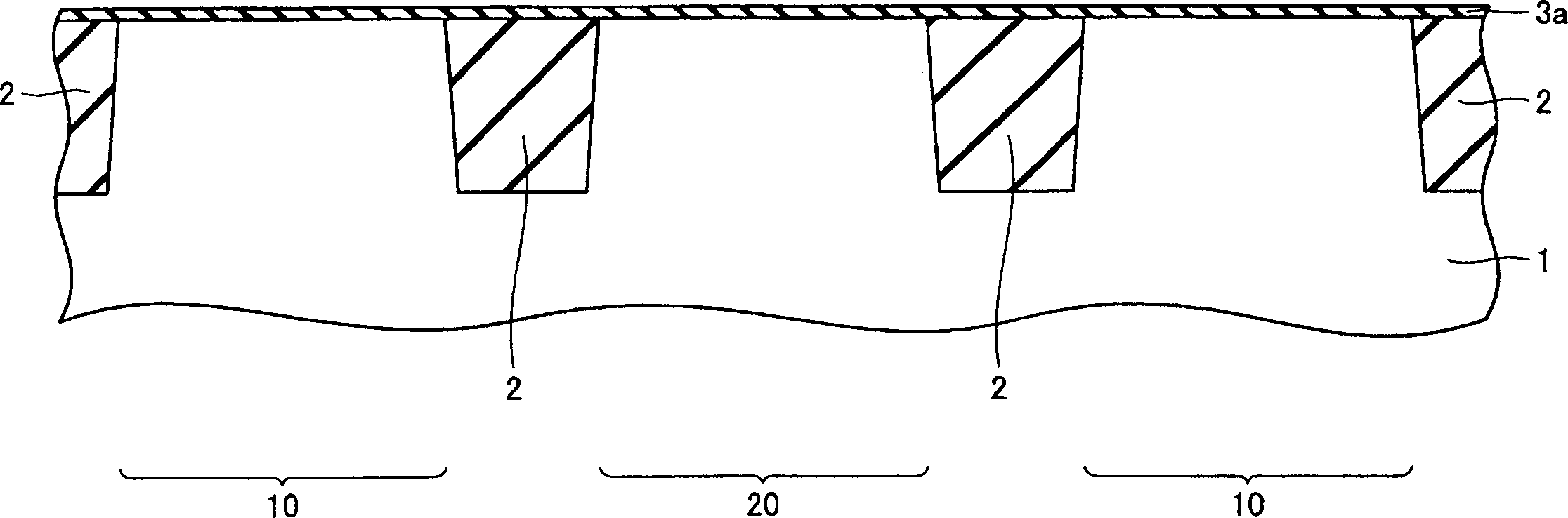
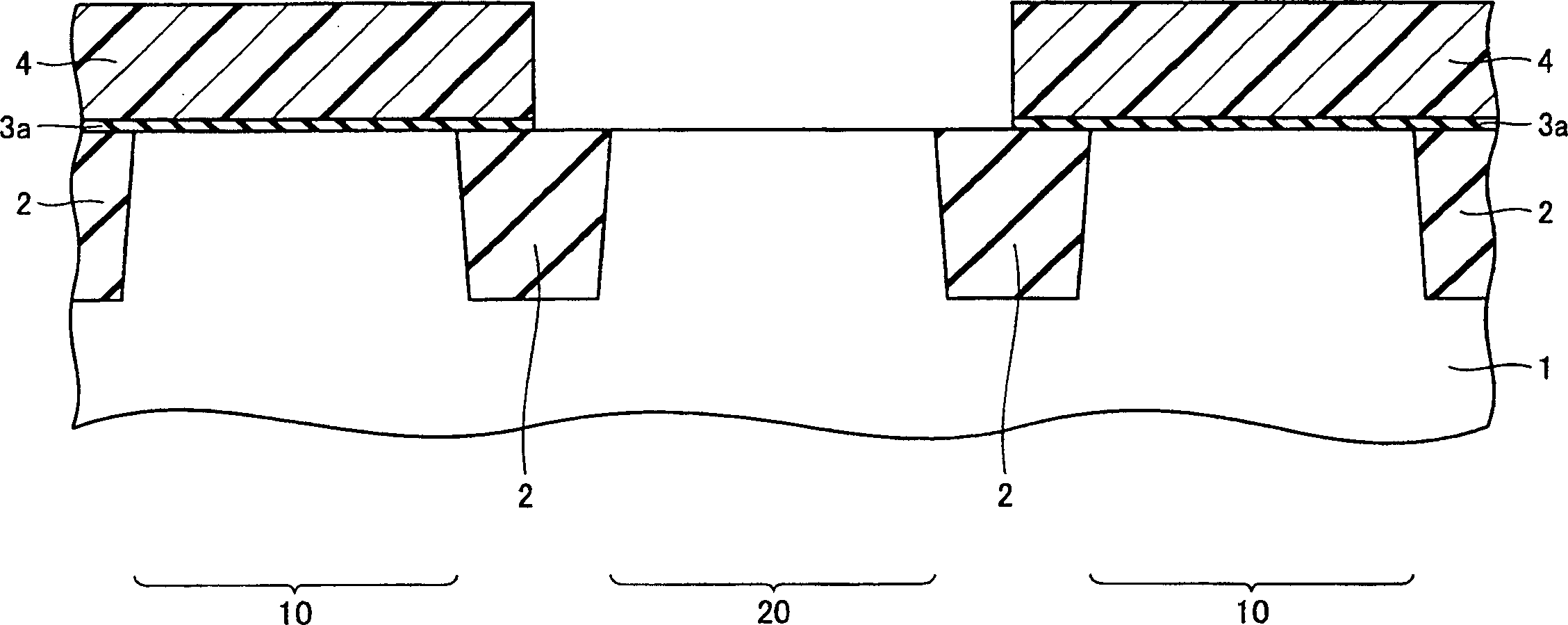
[0021] Such as figure 1 As shown, first, as a first step, a trench isolation film 2 is formed in a silicon substrate 1 as a semiconductor substrate to form a first active region 10 and a second active region 20. Here, the first active region 10 is a first electric field effect transistor 12 (refer to Figure 6 )Area. In addition, the second active region 20 is an electric field effect transistor 22 (refer to Figure 6 )Area.
[0022] As the first step, a normal STI structure manufacturing process can be adopted. Specifically, first, a pad oxide film is formed vertically above t...
PUM
| Property | Measurement | Unit |
|---|---|---|
| thickness | aaaaa | aaaaa |
| thickness | aaaaa | aaaaa |
Abstract
Description
Claims
Application Information