Check patentability & draft patents in minutes with Patsnap Eureka AI!

Semiconductor memory device

A semiconductor and device technology, applied in the field of semiconductor memory devices, can solve problems such as increased power consumption

Inactive Publication Date: 2004-12-01
SAMSUNG ELECTRONICS CO LTD
View PDF1 Cites 3 Cited by
  • Summary
  • Abstract
  • Description
  • Claims
  • Application Information

AI Technical Summary

Problems solved by technology

Therefore, conventional semiconductor devices have a problem of increased power consumption during write operations

Method used


Image

  • Semiconductor memory device
  • Semiconductor memory device
  • Semiconductor memory device

Examples


Embodiment Construction

[0019] Preferred embodiments of the present invention, examples of which are illustrated in the accompanying drawings, will now be described in detail.

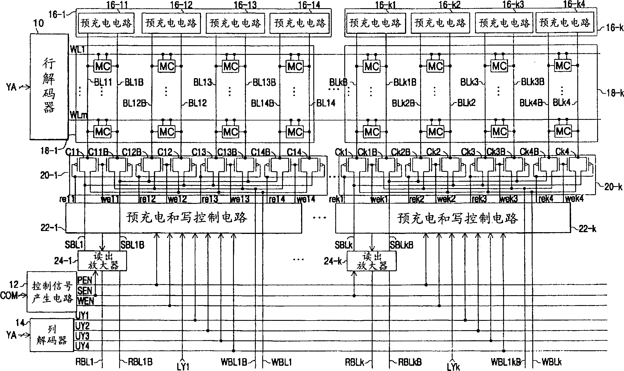
[0020] figure 1 is a block diagram of an example conventional semiconductor memory device. figure 1 The semiconductor memory device includes a row decoder 10, a control signal generation circuit 12, a column decoder 14, precharge circuits 16-1 to 16-k, memory cell array blocks 18-1 to 18-k, a column selection circuit 20-1 to 20-k, precharge and write control circuits 22-1 to 22-k, and sense amplifiers 24-1 to 24-k.

[0021] exist figure 1 Among them, each of the precharge circuits 16-1 to 16-k includes a precharge circuit for precharging the bit line pairs (BL11, BL11B) to (BL14, BL14B) to (BLk1, BLk1B) to (BLk4, BLk4B). Circuits (16-11~16-14) to (16-k1~16-k4). Each of the memory cell array blocks 18-1 to 18-k includes word lines WL1 to WLm and bit line pairs (BL11, BL11B) to (BL14, BL14B) to (BLk1, BLk1B) to (BLk4, BLk4B...


PUM


Abstract

Each memory block of a memory device a plurality of memory cells connected to a plurality of bit line pairs, a column selecting circuit, and a pre-charge and write control circuit. The column selecting circuit includes a plurality of CMOS transmission gates, each CMOS transmission gate including an NMOS transistor connected between one bit line of a bit line pair and a sense bit line of a sense bit line pair, and a PMOS transistor connected between the one bit line and one of the write bit lines of a write bit line pair. During a write operation, only the NMOS transistor of a selected one of the CMOS transmission gates is turned on, and the PMOS transistor of the selected CMOS transmission gate and the PMOS and NMOS transistors of all of the CMOS transmission gates except the selected one are all turned off.

Description

[0001] This application claims priority from Korean Patent Application No. 2003-11492 filed on February 24, 2003, the disclosure of which is hereby incorporated by reference in its entirety. technical field [0002] The present invention relates to a semiconductor storage device, more particularly, to a semiconductor storage device embedded in a system-on-chip (SOC, system-on-chip). Background technique [0003] Operations of a semiconductor memory device embedded in a conventional system-on-chip (SOC) include a precharge operation, a write operation, and a read operation. The precharge operation precharges bit line pairs and sense bit line pairs to a precharge voltage level in response to a precharge enable signal prior to write and read operations. The write operation writes data into the selected memory cell through the write bit line pair and the bit line pair in response to the write enable signal. The read operation reads data stored in the selected memory cell throug...

Claims


Application Information

Patent Timeline
Patent Type & Authority Applications(China)
IPC IPC(8): G11C7/00G11C7/10G11C7/12G11C7/22G11C11/34
CPCG11C2207/104G11C7/1006G11C7/22G11C2207/229G11C7/12G11C7/00
Inventor 朴仁圭
Owner SAMSUNG ELECTRONICS CO LTD
Features
  • R&D
  • Intellectual Property
  • Life Sciences
  • Materials
  • Tech Scout
  • Unparalleled Data Quality
  • Higher Quality Content
  • 60% Fewer Hallucinations
Learn More