Multilayer printed wiring board and integrated circuit using the same
A multi-layer printing and circuit board technology, applied in printed circuits, printed circuits, printed circuit manufacturing, etc., can solve problems such as ratio reduction, and achieve the effects of noise suppression, EMI improvement, and stable grounding
- Summary
- Abstract
- Description
- Claims
- Application Information
AI Technical Summary
Problems solved by technology
Method used
Image

Examples
Embodiment 1
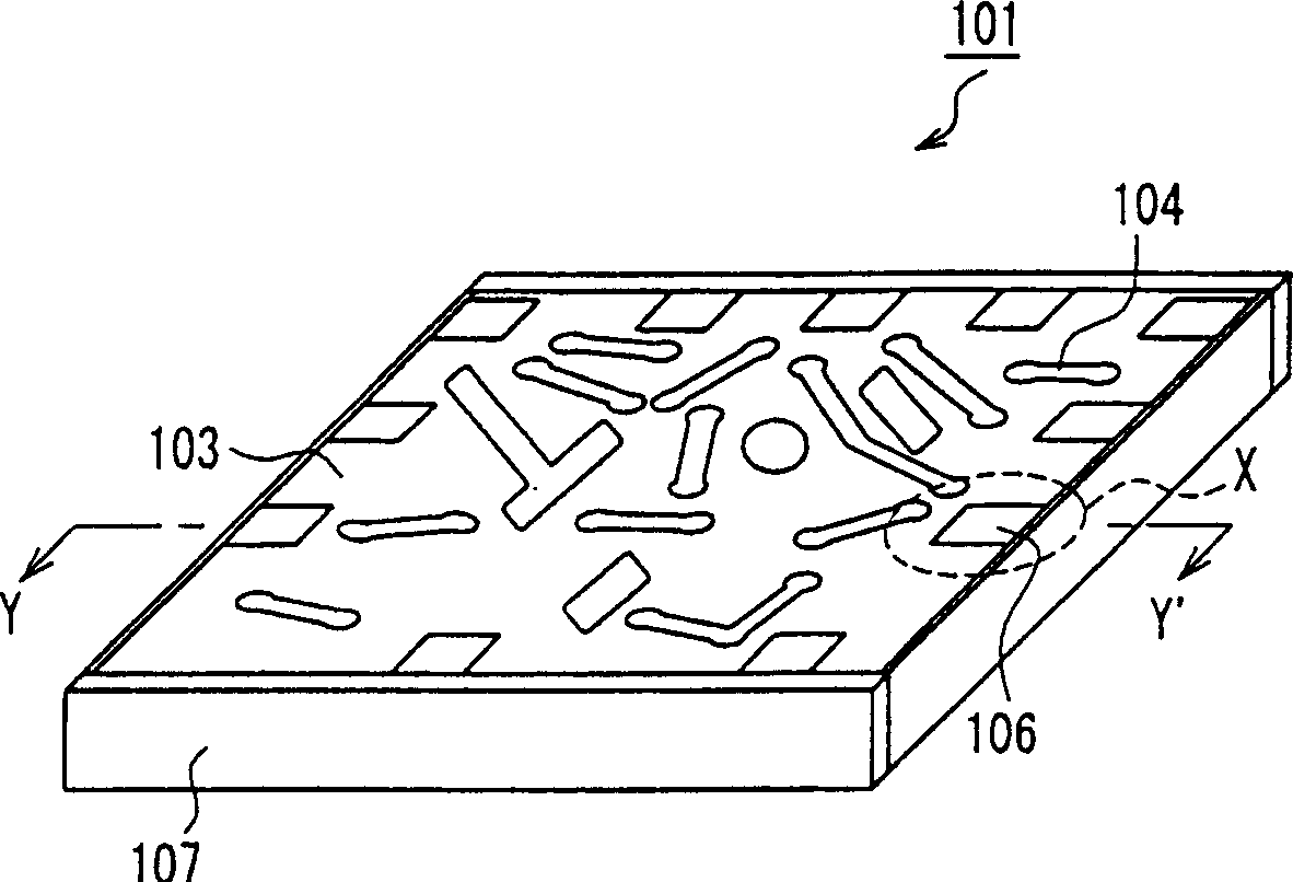
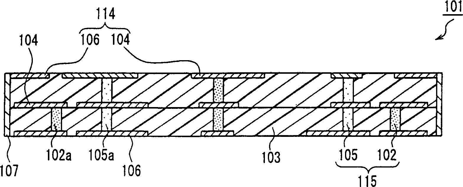
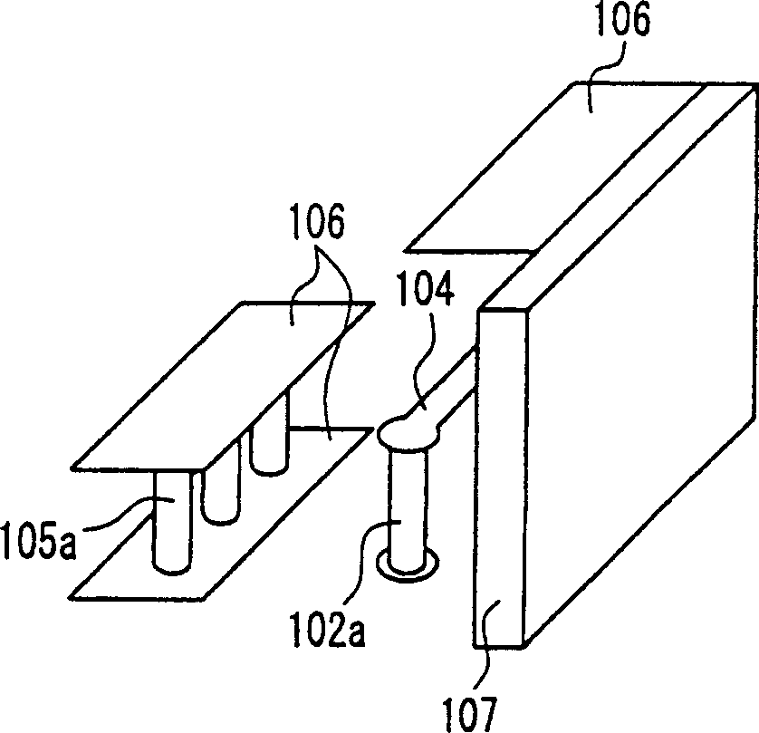
[0045] Figures 1A to 1D A multilayer printed wiring board of this embodiment is shown. Figure 1A It is a schematic perspective view of the principle. Figure 1B is along Figure 1A The cross-sectional view taken by the line Y-Y'. Figure 1D is another cross-sectional view. Figure 1C It is a schematic perspective view for explaining the internal structure of the multilayer printed wiring board and the impedance control structure.
[0046] Such as Figure 1A , 1B As shown in and 1D, the multilayer printed wiring board 101 includes a plurality of electrical insulating layers 103, a plurality of wiring layers 114 alternately arranged with the electrical insulating layers 103, and passes through each electrical insulating layer 103 along the thickness direction of the electrical insulating layer 103, A plurality of conductors 115 for electrically connecting the wiring layer 114 . Each wiring layer 114 includes ground lines 106 and signal transmission lines 104 . The conduct...
Embodiment 2
[0062] Figures 2A to 2C A multilayer printed wiring board of this embodiment is shown. Figure 2A is a cross-sectional view. Figure 2C is another cross-sectional view. FIG. 2B is a schematic perspective view for explaining an internal structural portion of the multilayer printed wiring board and an impedance control structure. The multilayer printed wiring board of this embodiment has the same effect as that of the multilayer printed wiring board of the first embodiment.
[0063] Such as Figure 2A and 2C As shown, the multilayer printed wiring board 209 includes a plurality of electrical insulation layers 203, a plurality of wiring layers 214 alternately arranged with the electrical insulation layers 203, passing through each electrical insulation layer 203 along the thickness direction of the electrical insulation layer 203, for electrical The plurality of conductors 215 connecting the wiring layer 214 and the circuit elements 208 buried in any electrical insulating l...
Embodiment 3
[0075] Figure 3A and 3B A sectional view showing the multilayer printed wiring board of this embodiment. Figure 3A The multilayer printed wiring board 309 in is the same as that of Embodiment 2, except that it further includes a material layer 311. Figure 3B The multilayer printed wiring board 309 in is the same as that of Embodiment 2, except that it also includes an electromagnetic shielding layer 312. The multilayer printed wiring board of this embodiment has effects comparable to those of the multilayer printed wiring boards of Embodiments 1 and 2.
[0076] Such as Figure 3A and 3B As shown, the multilayer printed wiring board 309 includes a plurality of electrical insulation layers 303, a plurality of wiring layers 314 alternately arranged with the electrical insulation layers 303, and a wire for passing through each electrical insulation layer 303 along the thickness direction of the electrical insulation layer 303. The plurality of conductors 315 of the wiring ...
PUM
 Abstract
Description
Claims
Application Information
 - R&D
- Intellectual Property
- Life Sciences
- Materials
- Tech Scout
- Unparalleled Data Quality
- Higher Quality Content
- 60% Fewer Hallucinations
Browse by: Latest US Patents, China's latest patents, Technical Efficacy Thesaurus, Application Domain, Technology Topic, Popular Technical Reports.
© 2025 PatSnap. All rights reserved.Legal|Privacy policy|Modern Slavery Act Transparency Statement|Sitemap|About US| Contact US: help@patsnap.com