Method for the production of thin layer chip resistors
一种薄膜芯片、电阻的技术,应用在电阻器、电阻制造、涂敷电阻材料等方向,能够解决单个电阻或电阻线路花费的时间长等问题
- Summary
- Abstract
- Description
- Claims
- Application Information
AI Technical Summary
Problems solved by technology
Method used
Image
Examples
Embodiment Construction
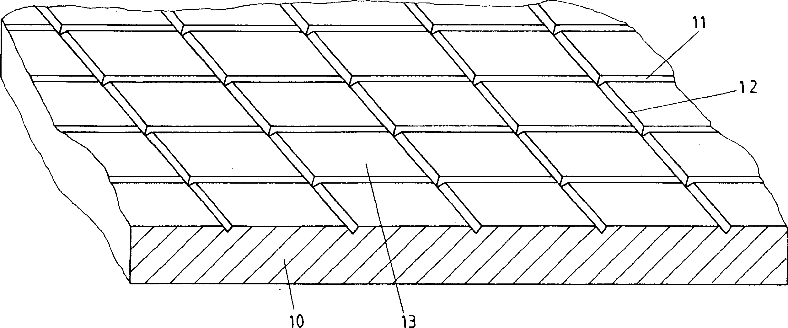
[0024] figure 1 The pregrooved, laser-scored or sawn substrate 10 which is preferably used in the production method according to the invention is reproduced in a perspective partial cutaway. The substrate 10 is made of, for example, glass, silicon, SiO, or an insulating ceramic such as Al 2 o 3 or AIN form. The upper side is divided into individual regions 13 by grooves 11 , 12 arranged perpendicularly to one another along a grid, in each region forming a thin-film chip resistor. The substrate 10 can also be sawn, or scribed with a laser, or not separated at all. Resistor arrays or resistor networks can also be formed according to the above divisions.
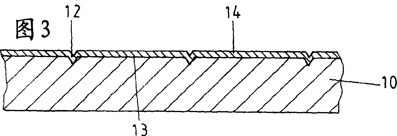
[0025] FIG. 2 again shows a longitudinal section of the substrate 10 on which a resistive layer 14 is first applied according to FIG. 3 , preferably over the entire surface of the substrate. The resistive layer 14 is usually a suitable resistive alloy, such as a metal layer composed of CrNi, CrSi, TaN, CuNi. The resistive...
PUM
| Property | Measurement | Unit |
|---|---|---|
| width | aaaaa | aaaaa |
| wavelength | aaaaa | aaaaa |
| wavelength | aaaaa | aaaaa |
Abstract
Description
Claims
Application Information
 - R&D
- Intellectual Property
- Life Sciences
- Materials
- Tech Scout
- Unparalleled Data Quality
- Higher Quality Content
- 60% Fewer Hallucinations
Browse by: Latest US Patents, China's latest patents, Technical Efficacy Thesaurus, Application Domain, Technology Topic, Popular Technical Reports.
© 2025 PatSnap. All rights reserved.Legal|Privacy policy|Modern Slavery Act Transparency Statement|Sitemap|About US| Contact US: help@patsnap.com


