Package for electronic parts, lid thereof, material for the lid and method for producing the lid material

A technology of electronic components and packages, which is applied in the direction of electrical components, electric solid devices, semiconductor/solid device parts, etc., can solve the problems of insufficient effect, low productivity of packages, poor welding operability, etc., and achieve operation Excellent performance, excellent airtightness, and the effect of suppressing cracking

Inactive Publication Date: 2005-01-05
DAISHINKU CORP +1
View PDF3 Cites 7 Cited by
  • Summary
  • Abstract
  • Description
  • Claims
  • Application Information

AI Technical Summary

Problems solved by technology

[0009] In the technology disclosed in Patent Document 2, it is recorded that copper foil is used as the deformation absorbing material of the cap or cap positioning device. Effective in preventing breakage of the plate-like substrate, but not sufficiently effective in preventing breakage of the thin-walled part of the miniaturized case
In addition, it is described that the copper foil is soldered to both sides of the substrate and the cap, but the soldering workability is poor, and the productivity of the package is also low.
[0010] On the other hand, in the technology disclosed in Patent Document 3, since the Ni-based metal and the solder material are laminated, only pressure bonding is performed, and there is no diffusion bonding. There are joint problems between the two layers when welding consumables

Method used


Image

  • Package for electronic parts, lid thereof, material for the lid and method for producing the lid material
  • Package for electronic parts, lid thereof, material for the lid and method for producing the lid material
  • Package for electronic parts, lid thereof, material for the lid and method for producing the lid material

Examples


Embodiment

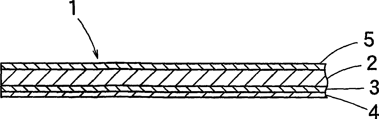
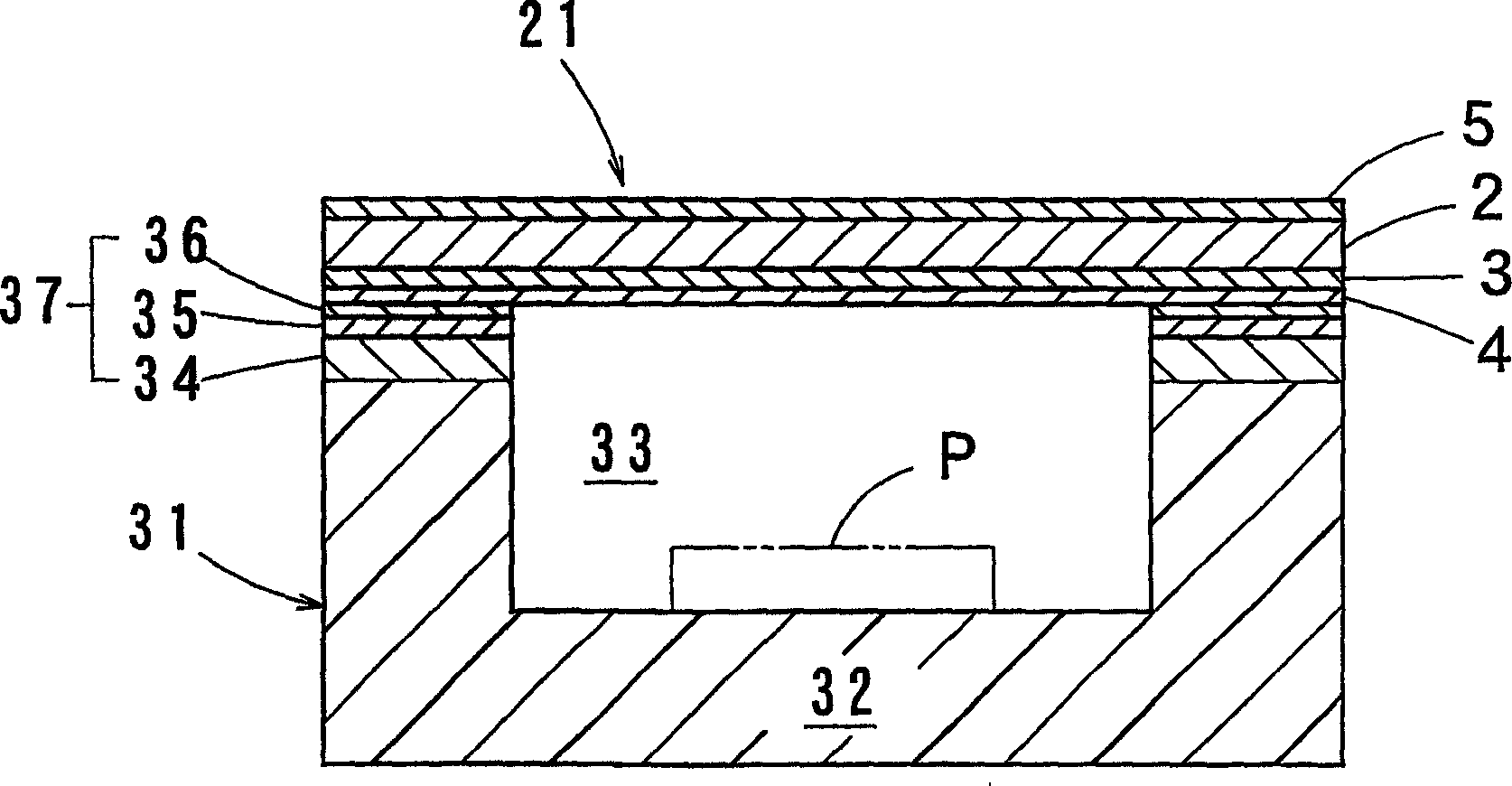
[0048] figure 1 The cover material sample of the shown 4-layer structure was produced by the following procedure. As the raw material of the substrate layer 2, a substrate sheet made of Fe-29 mass% Ni-17 mass% Co alloy with a width of 20 mm and a thickness of 1100 μm was prepared. As the Ni sheet made of Ni, a copper sheet made of oxygen-free copper (Cu: 99.95% by mass, O: 0.00006% by mass) with a width of 20 mm and a thickness of 600 μm was prepared as a raw material of the intermediate metal layer 3 . One surface of the base sheet is laminated with a nickel sheet, and the other surface is laminated with a copper sheet, and cold-compression bonding is carried out between rollers at a reduction rate of 60%, to obtain a copper bonded by pressure between adjacent materials. Layered layers. Furthermore, this copper laminate was held at 1000° C. for 3 minutes in an annealing furnace to perform diffusion annealing.

[0049] A solder material sheet formed of 85% by mass Ag-Cu (me...


PUM

PropertyMeasurementUnit
thicknessaaaaaaaaaa
melting pointaaaaaaaaaa
thicknessaaaaaaaaaa

Abstract

A lid material (1) according to the present invention comprises: a base layer (2) composed of a low thermal expansion metal; an intermediate metal layer (3) provided on one surface of the base layer (2) and composed of a low proof stress metal having a proof stress of not greater than 110 N / mm<2>; and a brazing material layer (4) provided on the intermediate metal layer (3) and composed of a silver brazing alloy mainly comprising silver. The intermediate metal layer (3) and the brazing material layer (4) are press- and diffusion-bonded to each other, and the brazing material layer (4) has a blistered area ratio of not greater than 0.5% as observed on an outer surface of the brazing material layer. The low proof stress metal is preferably oxygen-free copper. A lid produced from the lid material (1) exhibits an excellent bonding property when the lid is brazed to a case mainly composed of a ceramic material for an electronic component package. Further, the lid suppresses the breakage of the case, and ensures excellent brazing workability.

Description

technical field [0001] The present invention relates to a package for electronic components in which an opening of a case housing electronic components is sealed by a lid, the lid, and a lid material used as a raw material thereof. Background technique [0002] As disclosed in Japanese Unexamined Patent Application Publication No. 2000-3973 (Patent Document 1), a package for accommodating various electronic components such as a semiconductor element and a piezoelectric vibrator includes a case for accommodating electronic components with a concave portion opened on the upper surface thereof, and The cover body is welded to the outer peripheral portion of the opening of the case body so as to seal the concave portion and to block the opening portion of the case body. [0003] The aforementioned box body is formed of ceramics such as alumina or aluminum nitride as a main material. On the other hand, the cover body includes a base material layer formed of a low thermal expansi...

Claims


Application Information

Patent Timeline
Patent Type & Authority Applications(China)
IPC IPC(8): H01L23/10
CPCH01L2924/0002H01L23/10B32B15/018H01L2924/01079H01L2924/16195H01L2924/00H01L23/02
Inventor 盐见和弘石尾雅昭
Owner DAISHINKU CORP
Why Eureka
Try Eureka