Semiconductor device

Active Publication Date: 2014-11-27
FUJI ELECTRIC CO LTD
View PDF2 Cites 16 Cited by
  • Summary
  • Abstract
  • Description
  • Claims
  • Application Information

AI Technical Summary

Benefits of technology

[0026]According to embodiments of the present invention, the conductive block is disposed in the conductive pattern of the conductive-patterned insulating substrate to which the conductive block is fixed, such that the average volume per unit area of the conductive pattern around the section ther

Problems solved by technology

This leads to a problem in which the DCB substrate 104 and the sealing resin 111 peel off of each other.
This further increases the level of thermal

Method used


Image

  • Semiconductor device
  • Semiconductor device
  • Semiconductor device

Examples


example 1

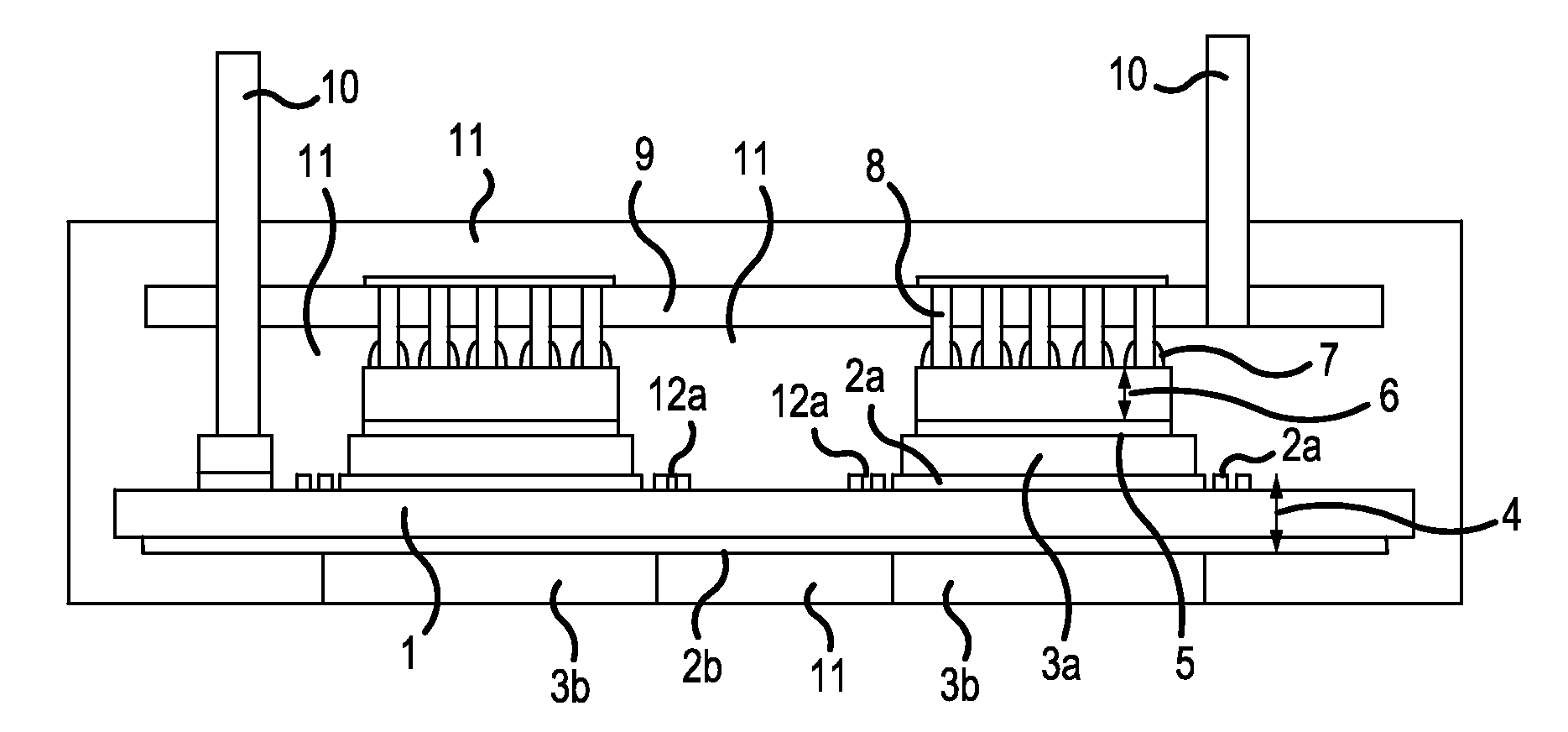
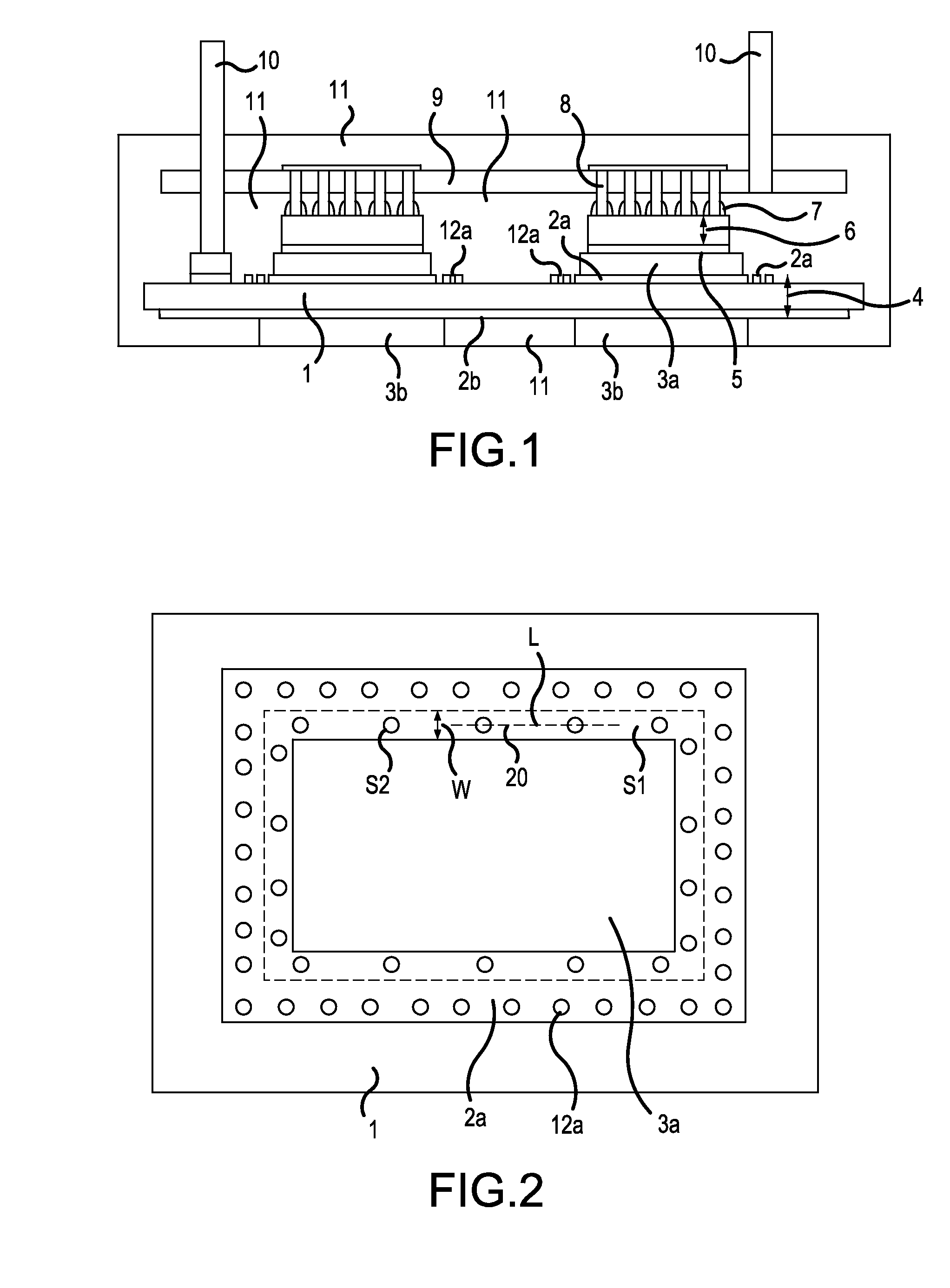
[0039]FIG. 1 is a cross-sectional diagram showing the principal parts of a semiconductor device according to a first example of the present invention. FIG. 2 is a plan view showing the principal parts of a DCB substrate shown in FIG. 1. In FIG. 1, a semiconductor power module, the semiconductor device, has a DCB (Direct Copper Bonding) substrate 4, which is a conductive-patterned insulating substrate configured by an insulating substrate 1 and copper circuit patterns 2a, 2b formed respectively on the front and back of the insulating substrate 1. This semiconductor module has copper blocks 3a fixed to the copper circuit patterns 2a of the DCB substrate 4 by diffusion bonding or the like, and copper blocks 3b fixed to the copper circuit pattern 2b of the DCB substrate 4 by diffusion bonding or the like. This semiconductor power module also has semiconductor chips 6 having the rear surfaces thereof soldered or the like onto the copper blocks 3a by bonding materials 5, conductive posts ...

example 2

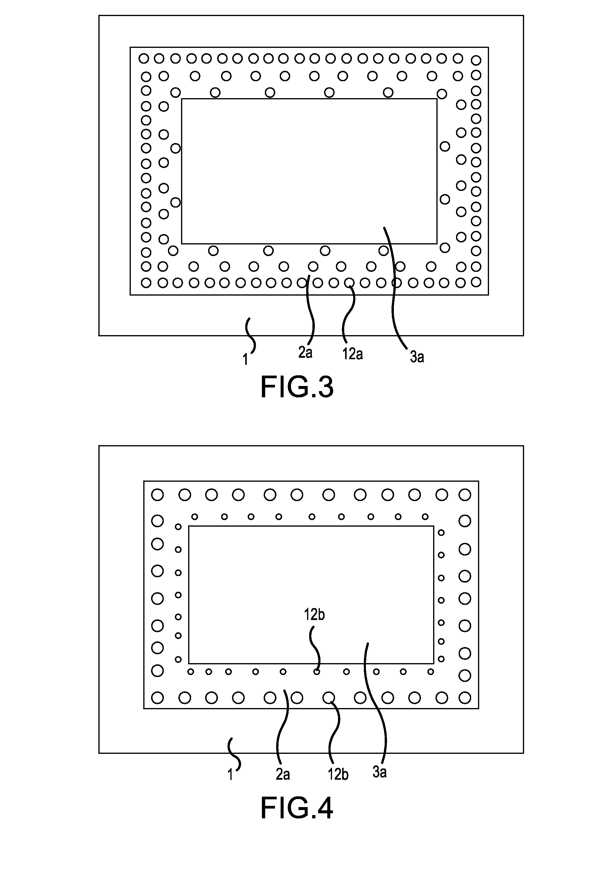
[0047]FIG. 4 is a plan view showing the principal parts of a semiconductor device according to a second example of the present invention. This diagram is a plan view of the principal parts of the DCB substrate 4 configuring the semiconductor device. This plan view corresponds to the plan view shown in FIG. 2.

[0048]The difference with FIG. 2 is that the size (cross-sectional area) of each drill hole 12b is changed while keeping the number of drill holes per unit area unchanged. The same effect as that described in Example 1 can be achieved by forming small drill holes 12b in the vicinity of each copper block 3a and large drill holes 12b away therefrom.

[0049]In both Examples 1 and 2, the drill holes 12a, 12b are in a circular shape; however, the shape of the drill holes is not limited thereto. Thus, rectangular drill holes 12c may be formed, as shown in FIG. 5. Alternatively, both rectangular and circular drill holes may be present.

example 3

[0050]FIG. 6 is a plan view showing the principal parts of a semiconductor device according to a third example. This diagram is a plan view showing the principal parts of the DCB substrate 4 configuring the semiconductor device. This plan view corresponds to the plan view shown in FIG. 2.

[0051]The difference with FIG. 2 is that the drill holes 12a to be formed are changed to annular drill grooves 12d. The number of annular drill grooves 12d per unit length in the direction from each copper block 3a toward the outside is increased toward the outside (so that the grooves are disposed densely), to reduce the area of the copper in the vicinity of the ceramic away from the copper block and increase the area of the copper in the vicinity of the copper block. With this configuration, the same effect as that of Example 1 can be achieved. The same effect can be obtained even by expanding the widths of drill grooves 12e toward the outside, as shown in FIG. 7. Although not shown, the annular d...


PUM


Abstract

A semiconductor device includes: a conductive-patterned insulating substrate; conductive blocks fixed to conductive patterns of the conductive-patterned insulating substrate; a semiconductor chip fixed to each conductive block; a printed circuit board that has a conductive post fixed to the semiconductor chip; and a resin. The semiconductor device is configured such that the average volume of a conductive film per unit area of each conductive pattern around a section thereof, to which the corresponding conductive block is fixed, is reduced from the conductive block toward the outside.

Description

CROSS REFERENCE TO RELATED APPLICATIONS[0001]This application is a continuation of International Application No. PCT / JP2013 / 053292, filed on Feb. 12, 2013, which is based on and claims priority to Japanese Patent Application No. JP 2012-058729, filed on Mar. 15, 2012. The disclosure of the Japanese priority application and the PCT application in their entirety, including the drawings, claims, and the specification thereof, are incorporated herein by reference.BACKGROUND[0002]1. Field of the Invention[0003]Embodiments of the present invention relate to a semiconductor device such as a power semiconductor module.[0004]2. Discussion of the Background[0005]FIG. 11 is a cross-sectional diagram showing the principal parts of a conventional semiconductor device having a structure similar to the one described in Japanese Patent Application Laid-open No. 2009-64852 (“Patent Document 1”). A power semiconductor module as the conventional semiconductor device has a DCB (Direct Copper Bonding) s...

Claims


Application Information

Patent Timeline
IPC IPC(8): H05K1/02H05K1/11H05K1/18
CPCH05K1/0296H05K1/185H05K2201/098H05K2201/09609H05K2201/09727H05K1/115H01L23/3121H01L23/3735H01L23/4334H01L23/49811H01L23/49833H01L25/072H01L24/01H01L2924/351H01L2924/15747H01L2924/15787Y02E10/50H01L2924/00H01L23/28H01L31/048H01L33/56H01L23/12H01L33/52H01L21/563H01L21/56
Inventor NAKAMURA, YOUKONASHIDA, NORIHIRO
Owner FUJI ELECTRIC CO LTD
Why Eureka
Try Eureka