Switching device

A technology of switching devices and devices, which is applied in the direction of semiconductor devices, electrical components, engine components, etc., and can solve problems such as difficult to manufacture devices

Inactive Publication Date: 2005-01-05
バーンズリミテッド
View PDF0 Cites 3 Cited by
  • Summary
  • Abstract
  • Description
  • Claims
  • Application Information

AI Technical Summary

Problems solved by technology

[0006] Simple glass-passivated PNPN devices are commonly used for switching devices, but it is difficult to fabricate such devices with the required capacitance limit

Method used


Image

  • Switching device
  • Switching device
  • Switching device

Examples


Embodiment Construction

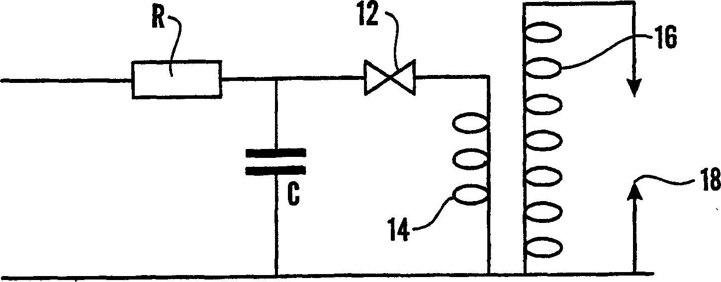
[0023] refer to figure 1 , the figure shows a simple spark generator circuit 10 in which a capacitor C is charged by a supply voltage through a resistor R. The circuit has a PNPN bidirectional semiconductor switching device 12 which is triggered into electrical conduction when the voltage across capacitor C exceeds the turn-on voltage of device 12 . This discharges the capacitor through the primary winding 14 of the step-up transformer. The transformer develops a very high voltage across its secondary winding 16 which creates a spark between spark gaps 18 .

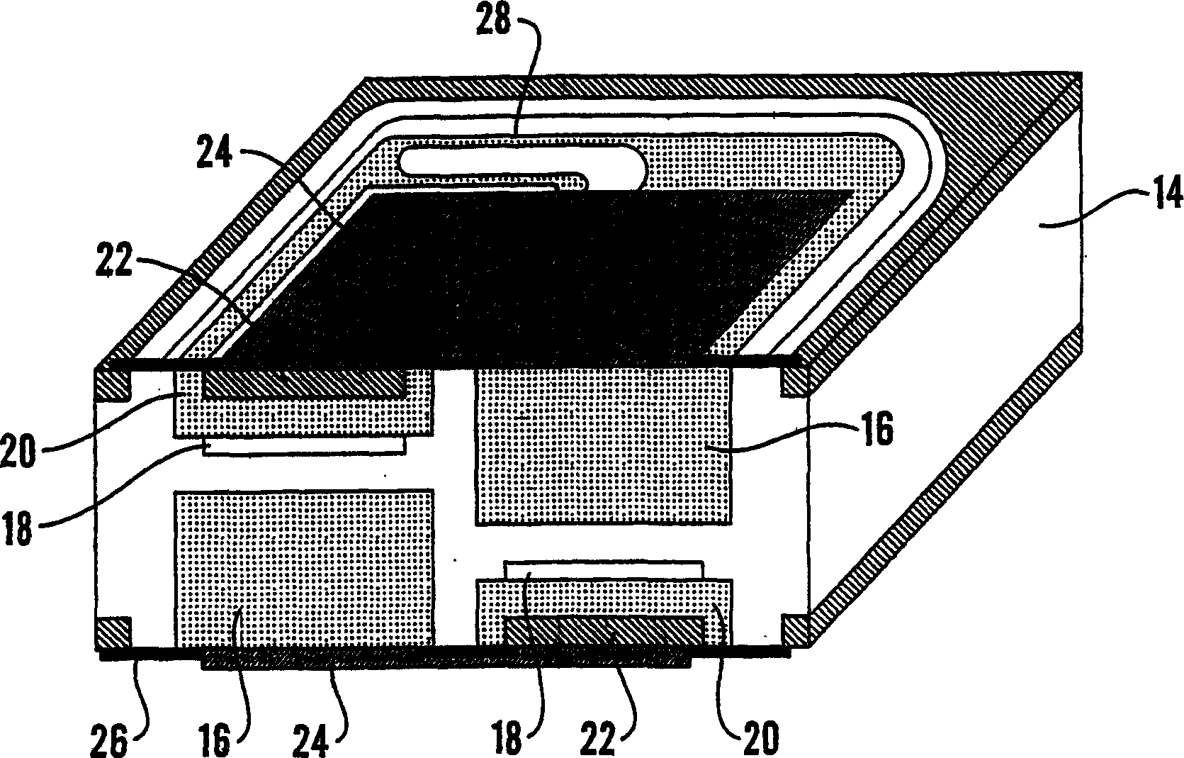
[0024] refer to figure 2 , the figure shows that according to the present invention will use figure 1 A cross-sectional view of a preferred embodiment of the semiconductor switching device 12 of the middle circuit.

[0025] figure 2 The device shown in is a bidirectional PNPN device having an N-type substrate 14 . The P-type deep anode region 16 is formed by diffusion on the opposite side of the N-type substrate. ...


PUM


Abstract

A PNPN semiconductor switching device for igniter circuits comprises first (22) and third (14) diffusion layers of N-type conductivity semiconductor material, second (20) and fourth (16) diffusion layers of P-type conductivity type semiconductor material, and a first buried region (18) of N-type conductivity in the third layer (14) adjacent to the junction between the second (20) and third (14) layers. The buried region has a greater impurity concentration than the third layer (18) and serves to control the switching voltage of the device. The first to third diffusion layers form an NPN transistor (TR1) and a resistance (28) is formed as part of the transistor base diffusion between the base and emitter diffusion regions (20, 22) of the transistor (TR1) for controlling the switching current of the device.

Description

technical field [0001] This invention relates to switching devices for use in spark generator circuits. Background technique [0002] Bi-directional silicon switching devices are often used in spark or pulse generator circuits, for example to ignite gas appliances or to start lamps, etc. [0003] In common circuits, supply voltage is used to charge capacitors. When the breakover voltage of the silicon switching device is exceeded, the device triggers to conduct and discharges the capacitor through the primary winding of the step-up transformer. The transformer produces a very high voltage across its secondary winding, which then passes through the spark gap to create a spark. This spark is used to ignite gas appliances. [0004] Such a circuit can also be used to generate the high voltage needed to ignite a gas discharge tube shaped bulb. In the case of high intensity discharge (HID) lamps, multiple (eg at least three) ignition pulses need to be provided for each mains h...

Claims


Application Information

Patent Timeline
Patent Type & Authority Applications(China)
IPC IPC(8): F02P3/04H01L29/747H01L29/861
CPCF02P3/0435H01L29/747F02D2041/2075
Inventor 昆瑞德·吕特赫斯斯蒂芬·威尔顿·拜厄特
Owner バーンズリミテッド
Why Eureka
Try Eureka