Device and method for nondestructive inspection on semiconductor device

A non-destructive, semiconductor technology, applied in semiconductor/solid-state device testing/measurement, electrical components, non-contact circuit testing, etc.

Inactive Publication Date: 2005-01-26
NEC ELECTRONICS CORP
View PDF7 Cites 3 Cited by
  • Summary
  • Abstract
  • Description
  • Claims
  • Application Information

AI Technical Summary

Problems solved by technology

[0043] The second problem is that even if the detection is performed after the formation of the pads is completed so that the post-processing process of the manufacturing is completed, since there are a large number of pads connected to the current change detector, many work steps and a lot of cost are required in order to prepare for the establishment of the electrical connection.
However, the probability of two types of defects existing on the same metal line is very small

Method used


Image

  • Device and method for nondestructive inspection on semiconductor device
  • Device and method for nondestructive inspection on semiconductor device
  • Device and method for nondestructive inspection on semiconductor device

Examples


Embodiment A

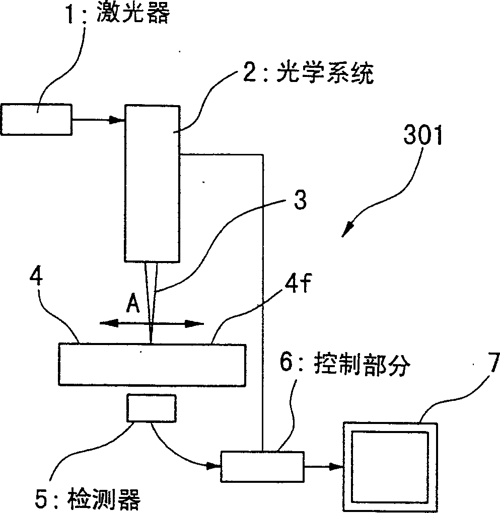
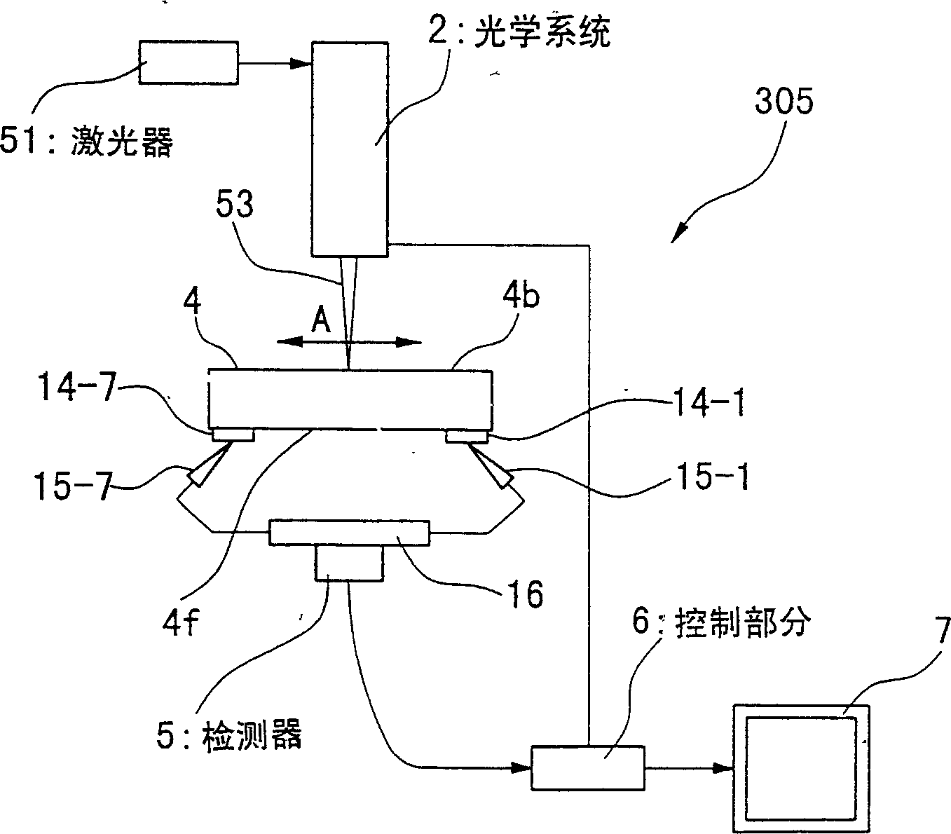
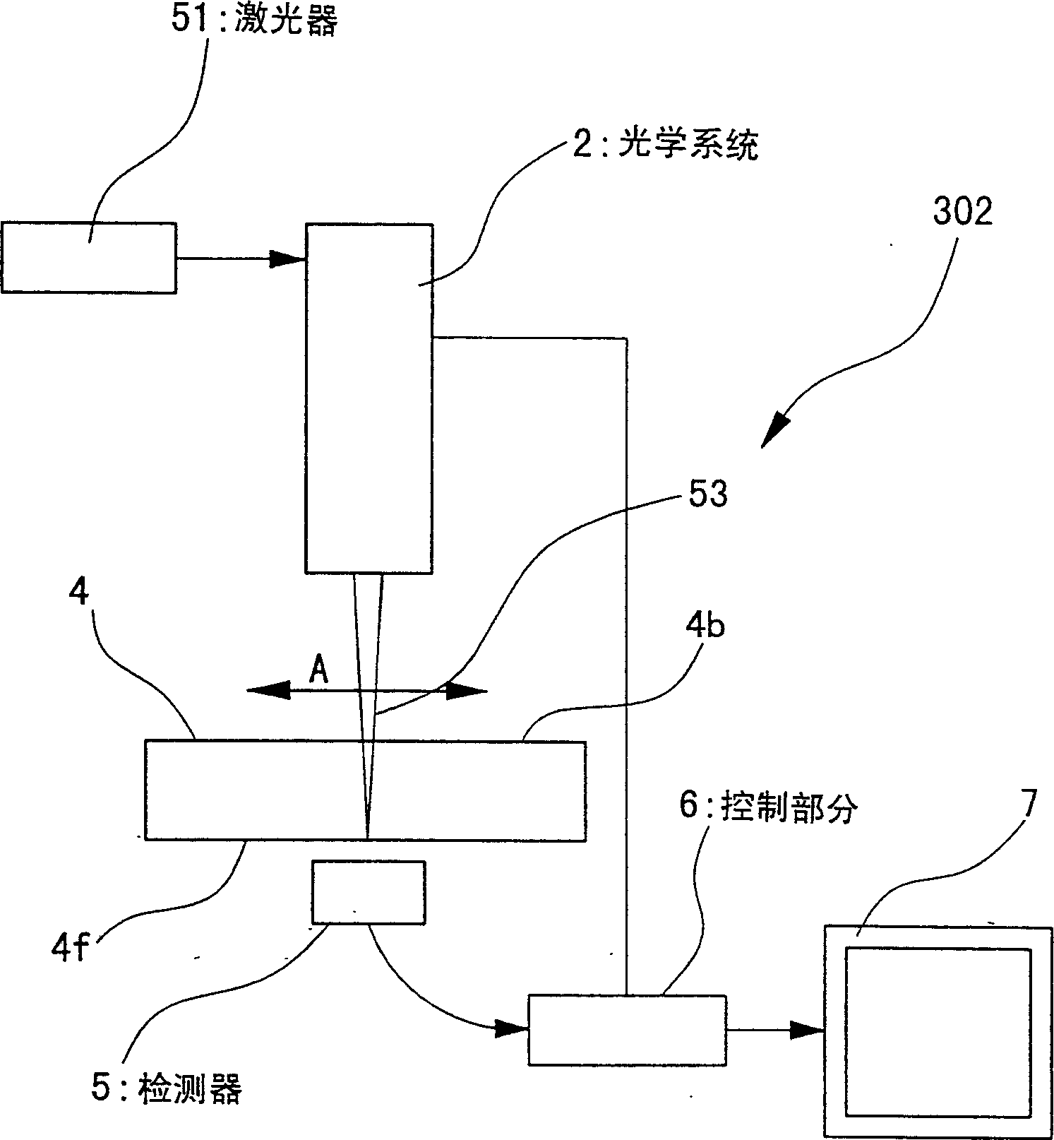
[0101] Embodiment A contains various examples designed for non-destructive inspection in accordance with the present invention.

[0102] Figure 1A , 1B , 2, 3 and 4 are five examples showing the non-destructive inspection apparatus according to Embodiment A of the invention, which are similar to those shown in Figure 8 and 9 Equivalent and identical parts are assigned the same reference numerals.

[0103] Now, refer to Figure 1A , 2 , 3 and 4 describe examples 1, 2, 3 and 4 of the non-destructive inspection device in sequence. Here, the structures of those examples will be described first, and then, the operation procedures will be described.

[0104] exist Figure 1A The non-destructive inspection device 301 of the illustrated example 1 is configured as follows:

[0105] Laser 1 produces a laser beam, which is narrowed in irradiation size by optical system 2 to produce laser beam 3 . The laser beam 3 is irradiated on the upper surface 4f of the semiconductor device...


PUM


Abstract

A nondestructive inspection device (or method) is basically configured such that a laser beam (1300 nm) (3, 53) is irradiated on a surface (or back) of a semiconductor device chip to scan. Due to irradiation of the laser beam, a defect position is heated to cause a thermoelectromotive current, which induces a magnetic field. A magnetic field detector (5) such as SQUID (55) detects a strength of the magnetic field, based on which a scan magnetic field image is produced. A display device (7) superimposes the scan magnetic field image on a scan laser microphotograph on a screen, so it is possible to perform defect inspection on the semiconductor device chip. Incidentally, a semiconductor device wafer (40) is constructed to include a thermoelectromotive force generator (21) and its wires (20a).

Description

technical field [0001] The present invention relates to apparatus and methods for non-destructive inspection of chips of semiconductor devices, and in particular to non-destructive inspection for detection of electrical defects. The present invention also relates to a semiconductor device suitable for non-destructive inspection, and a method of manufacturing the same. [0002] This application is based on Patent Application Hei 10-272788, Patent Application Hei 11-67744 and Patent Application Hei 11-133283 filed in Japan, the contents of which are incorporated herein. Background technique [0003] The usual non-destructive inspection techniques are described by known contributions such as the title "Thermal Electromotive Force-Based OBIC Analysis Technique", which was presented as material for the 132 meeting of the Research Aspects of the Japan Research Institute Promotion Fund 132 Committee on Charged Particles industrial applications. Here, "OBIC" is an abbreviation for...

Claims


Application Information

Patent Timeline
Patent Type & Authority Applications(China)
IPC IPC(8): H01L21/66G01R31/303G01R31/308G01R31/311
CPCG01R31/311H01L22/00
Inventor 二川清
Owner NEC ELECTRONICS CORP
Why Eureka
Try Eureka