

Thermally enhanced component substrate
A technology for substrates and heat-conducting components, applied in semiconductor/solid-state device parts, electrical components, electric solid-state devices, etc.
- Summary
- Abstract
- Description
- Claims
- Application Information
AI Technical Summary
Problems solved by technology
Method used
Image

Examples
Embodiment Construction
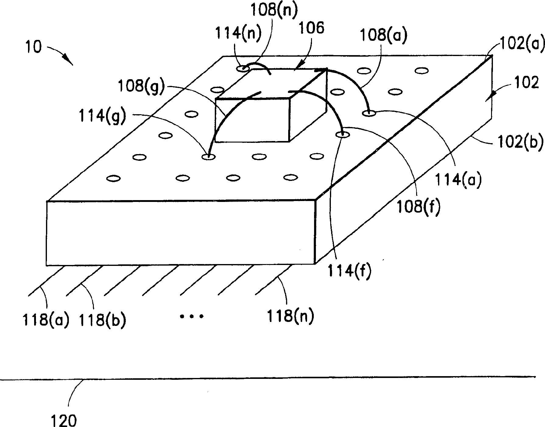
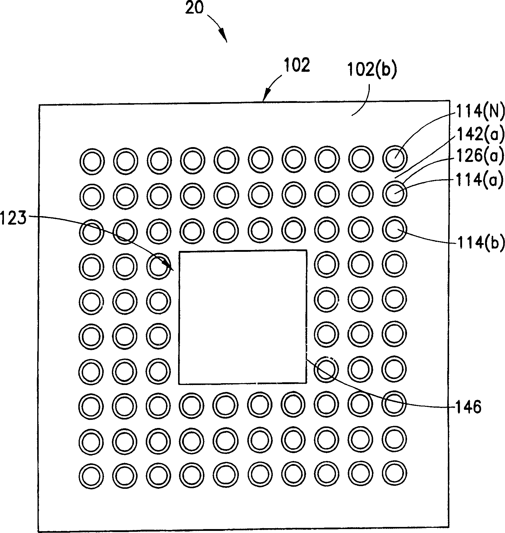
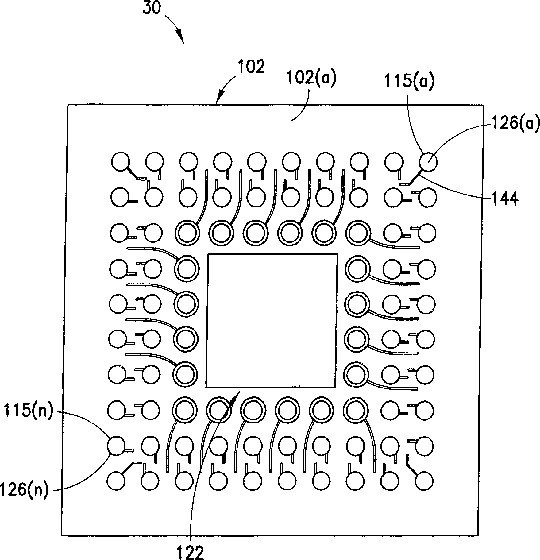
[0024] For both integrated circuit packages and MCM components, the present invention addresses the need to make the thermally active area from the die to the printed circuit board (PCB) The thermal resistance is minimized. The present invention is particularly useful in applications requiring enhanced thermal passage from the die to the solder balls, especially in applications where there is no overlap between the die and the solder balls, such as in BGA (Ball Grid Array ) packages without center ball peripheral pins (for example, Tessera uBGA, STLF- and TFBGA, etc.).
[0025] The present invention integrates thermal and electrical functions into the same pin. In particular, I / O pins that do not overlap the die can be thermally connected to the die by using a thermally conductive element, such as copper, between the pin and the underside of the die. A pin can be under the die, or it can be a peripheral pin. The central heat bulb can also have an electrical function. Thus,...
PUM
 Abstract
Description
Claims
Application Information