Method of fabricating micro-electromechanical switches on cmos compatible substrates

A technology of micro-electronic machinery and switches, applied in the field of MEMS manufacturing

Inactive Publication Date: 2005-02-02
格芯公司
View PDF4 Cites 24 Cited by
  • Summary
  • Abstract
  • Description
  • Claims
  • Application Information

AI Technical Summary

Problems solved by technology

This is too high for applications like mobile p

Method used


Image

  • Method of fabricating micro-electromechanical switches on cmos compatible substrates
  • Method of fabricating micro-electromechanical switches on cmos compatible substrates
  • Method of fabricating micro-electromechanical switches on cmos compatible substrates

Examples


Embodiment Construction

[0034] The main embodiments teach the fabrication of MEMS devices by methods that can be fully integrated with standard CMOS, bipolar, BiCMOS or other common semiconductor chip processes.

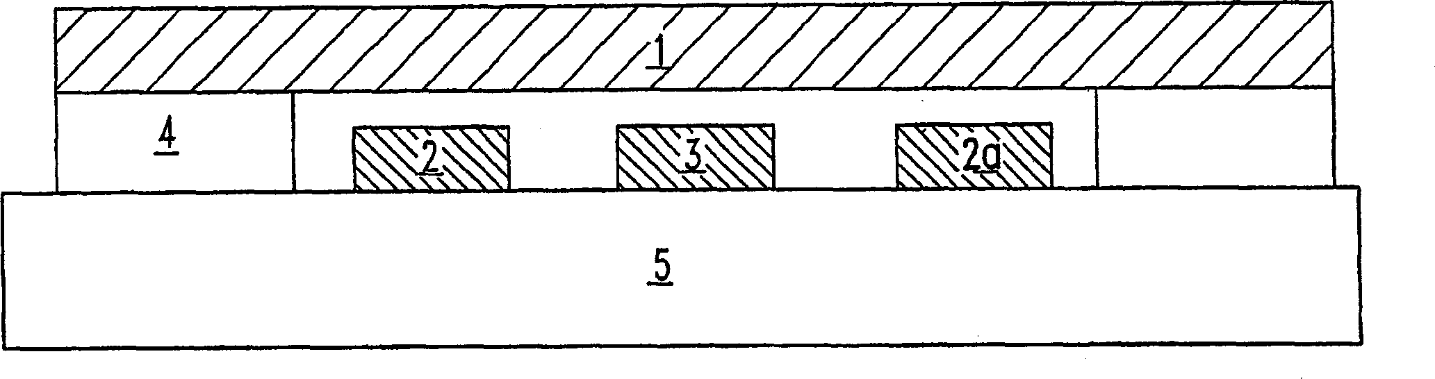
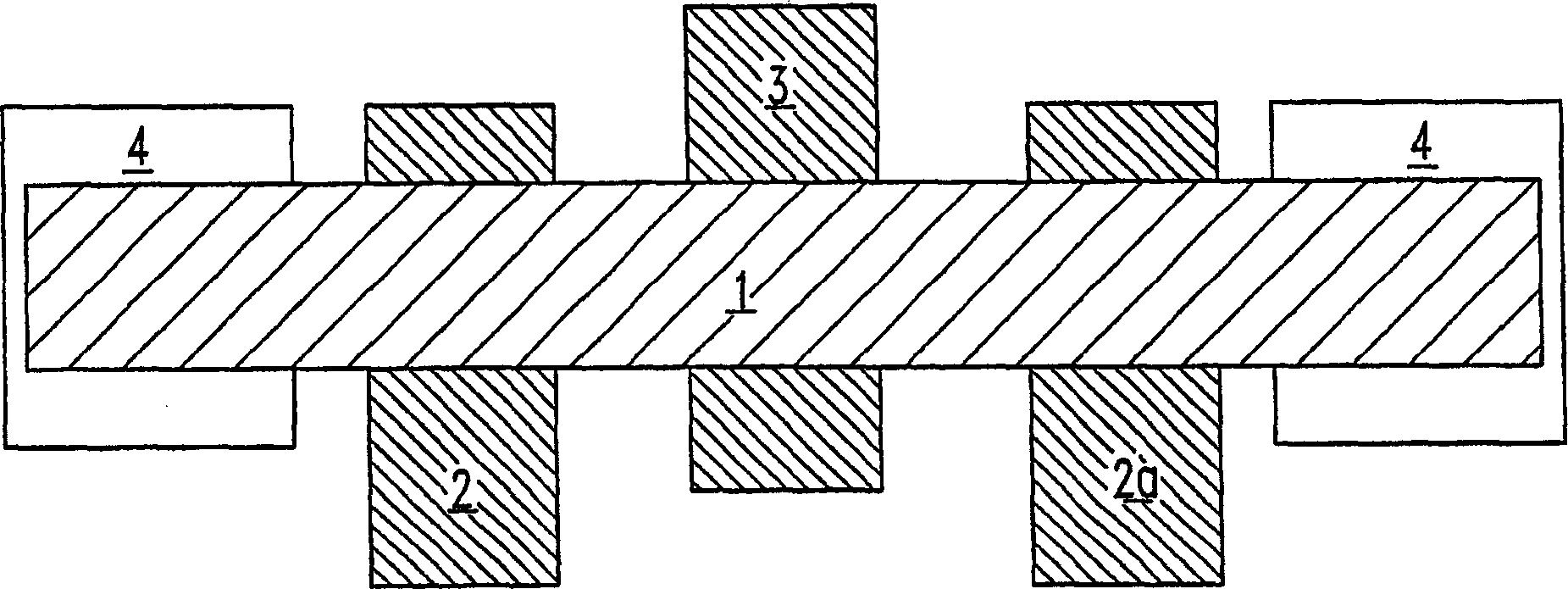
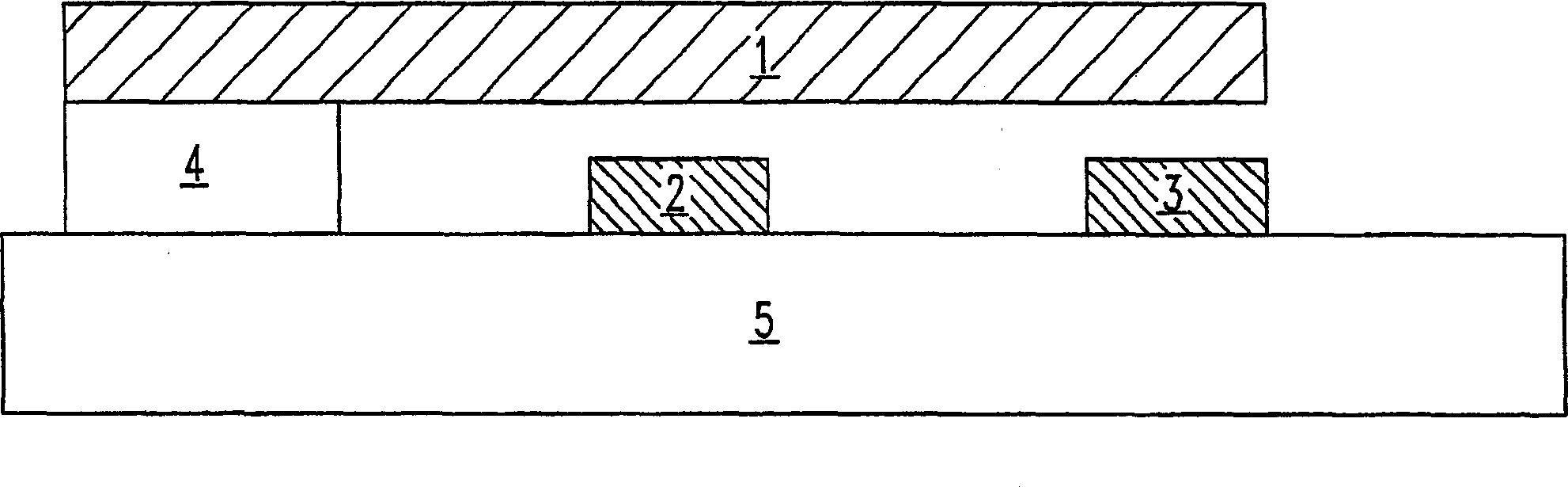
[0035] Figure 5 The initial structure, the copper damascene interconnect layer, is illustrated. Below this, on a silicon substrate or alternatively on a preferably SiO 2 Devices such as FETs, NPN transistors or HBT (Hetero-junction Bipolar Transistors, heterojunction bipolar transistors), resistors, etc. can be placed on the fabricated low-loss substrate. It consists of embedding in preferably SiO 2 The copper wirings 30, 40, and 50 in the dielectric layer 20 constituted. The area indicated by reference numeral 30 represents the landing metal for the via 110 buried in the dielectric layer 100 . The metal designated by reference numeral 40 forms the actuator or control electrode, and the metal 50 represents the signal electrode. The thickness of the metal is generally on the order of 3...


PUM


Abstract

A method of fabricating micro-electromechanical switches (MEMS) integrated with conventional semiconductor interconnect levels, using compatible processes and materials is described. The method is based upon fabricating a capacitive switch that is easily modified to produce various configurations for contact switching and any number of metal-dielectric-metal switches. The process starts with a copper damascene interconnect layer, made of metal conductors inlaid in a dielectric. All or portions of the copper interconnects are recessed to a degree sufficient to provide a capacitive air gap when the switch is in the closed state, as well as provide space for a protective layer of, e.g., Ta/TaN. The metal structures defined within the area specified for the switch act as actuator electrodes to pull down the movable beam and provide one or more paths for the switched signal to traverse. The advantage of an air gap is that air is not subject to charge storage or trapping that can cause reliability and voltage drift problems. Instead of recessing the electrodes to provide a gap, one may just add dielectric on or around the electrode. The next layer is another dielectric layer which is deposited to the desired thickness of the gap formed between the lower electrodes and the moveable beam that forms the switching device. Vias are fabricated through this dielectric to provide connections between the metal interconnect layer and the next metal layer which will also contain the switchable beam. The via layer is then patterned and etched to provide a cavity area which contains the lower activation electrodes as well as the signal paths. The cavity is then back-filled with a sacrificial release material. This release material is then planarized with the top of the dielectric, thereby providing a planar surface upon which the beam layer is constructed.

Description

technical field [0001] The present invention relates generally to the fabrication of micro-electromechanical switches (MEMS), and more particularly to MEMS fabrication that can be integrated with the current state of the art semiconductor fabrication process technology. Background technique [0002] Switching is a fundamental part of many electronic, mechanical and electromechanical applications. MEM switches have attracted considerable attention over the past few years. Products using MEMS technology are common in biomedical, aerospace and communication systems. [0003] Traditional MEMS generally utilize cantilever switches, membrane switches, and adjustable capacitance structures, such as in McMillan et al. US Patent No. 6,160,230, Feng et al. US Patent No. 6,143,997, Carley et al. described in U.S. Patent No. 5,880,921. MEMS devices are fabricated using microelectromechanical technology and are used to control the flow of electrical, mechanical or optical signals. Bu...

Claims


Application Information

Patent Timeline
IPC IPC(8): B81B3/00B81C1/00H01H49/00H01H59/00
CPCB81B2203/0127H01G5/40B81C2201/0122H01H59/0009B81B2201/018B81C2203/0735B81C1/00246B81B2201/016B81B2207/07B81C1/00611H01L29/00
Inventor 理查德·P·沃兰特约翰·C·比森唐娜·R·科特蒂莫西·J·多尔顿罗伯特·A·格罗夫斯凯文·S·皮特拉卡肯尼思·J·斯坦塞沙德里·苏班纳
Owner 格芯公司
Why Eureka
Try Eureka