Electron beam processing apparatus

An electron beam processing, positive ion technology, applied in the directions of irradiation devices, ion beam tubes, circuits, etc., can solve the problems of reducing the cooling effect, the acceleration grid 3 cannot obtain sufficient cooling effect, and the contact area is reduced, etc.

Inactive Publication Date: 2005-02-09
MURATA MFG CO LTD
View PDF1 Cites 5 Cited by
  • Summary
  • Abstract
  • Description
  • Claims
  • Application Information

AI Technical Summary

Problems solved by technology

[0012] However, in this case, since the contact area between the cooling jacket 5 and the acceleration grid 3 is reduced, there is a disadvantage that the acceleration grid 3 cannot obtain a sufficient cooling effect.
Especially since the inner edge of the opening of the cooling jacket 5 is far away from the porous part 3a of the acceleration grid 3 with the highest temperature, the cooling effect is reduced.

Method used


Image

  • Electron beam processing apparatus
  • Electron beam processing apparatus
  • Electron beam processing apparatus

Examples


Embodiment Construction

[0031] Hereinafter, specific embodiments of the present invention will be described with reference to examples.

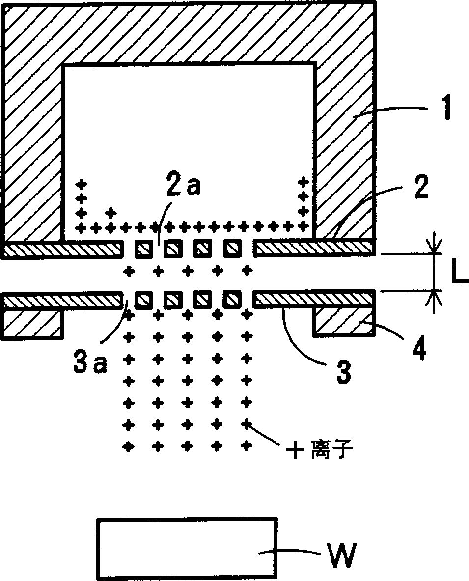
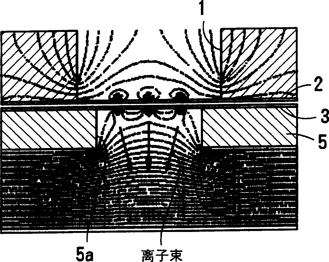
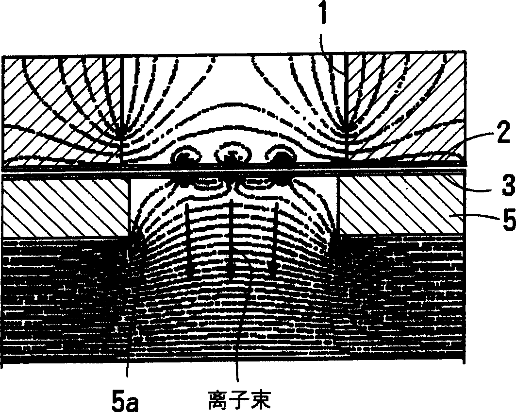
[0032] Figure 4 , Figure 5 An example of the electron beam processing apparatus of the present invention is shown. Figure 4 versus figure 1 The same parts are represented by the same symbols and will not be repeated.

[0033] In this processing device, the cooling jacket 5 on the front side of the acceleration grid 3 is tightly fixed by screws or the like. A cooling water channel 5b is formed inside the cooling jacket 5, which has the function of absorbing the heat conducted from the acceleration grid 3 to the cooling jacket 5 and removing it to the outside.

[0034] The cooling jacket 5 is formed with an opening 5a wider than the range in which the fine hole 3a of the acceleration grid 3 is provided. The opening 5a, such as Figure 5 As shown, the pores 3a of the acceleration grid 3 arranged in a rectangular shape correspond to the pores 3a, and are elliptical, a...


PUM


Abstract

Provided is an electron beam processing device capable of preventing deviation of an ion beam to the center, and of keeping a cooling effect of an acceleration grid. This electron beam processing device is equipped with: a plasma generation chamber 1; a shielding grid 2 mounted on the front surface of an opening of the plasma generation chamber; the acceleration grid 3 disposed in front of the shielding grid with a space; and a cooling jacket 5 mounted on the front surface of the acceleration grid 3 and having an opening 5a wider than a range where fine pores 3a of the acceleration grid 3 are formed. By forming the opening 5a of the cooling jacket 5 into a shape gradually expanded toward the traveling direction of the ion beam, an equipotential line is set nearly parallel to the acceleration grid 3, so that deviation of the ion beam to the center can be restrained and the cooling effect to the acceleration grid 3 can be kept.

Description

Technical field [0001] The invention relates to an electron beam processing device for etching with ion beams. Background technique [0002] [Patent Document 1] JP 2002-75232 A [0003] In the past, electron beam processing devices that use ion beams to trim metal films or oxide films formed on electronic components such as piezoelectric resonators to adjust their electrical characteristics have been widely known. [0004] figure 1 To show the basic principle of an electron beam processing device that generates an electron beam. In the figure, 1 is a plasma generation chamber, 2 is a screen grid with multiple pores 2a, 3 is an acceleration grid with multiple pores 3a corresponding to the pores 2a of the screen grid 2, and 4 is The accelerating grid base of the accelerating grid 3 is maintained. The outer periphery of the screen grid 2 is fixed to the plasma generation chamber 1, the outer periphery of the acceleration grid 3 is fixed to the acceleration grid base 4, and the acc...

Claims


Application Information

Patent Timeline
Patent Type & Authority Applications(China)
IPC IPC(8): H01J27/02G21K5/04H01J27/14H01J37/08H01L21/302H05H1/24
CPCH01J27/024H01J27/14H01J27/143H01L21/3065
Inventor 池田功尾岛茂夫
Owner MURATA MFG CO LTD
Why Eureka
Try Eureka