Manufacturing method for electronic component-mounted component, manufacturing method for electronic component-mounted completed product with the electronic component-mounted component, and electronic component-mounted completed product

a manufacturing method and electronic component technology, applied in the direction of printed circuit non-printed electric components association, conductive pattern formation, instruments, etc., can solve the problems of increasing module size, inability to respond to the latest need for products to be thinned, and prone to bending, etc., to achieve high functionality, reduce thickness of electronic component-mounted components, and small in size

Inactive Publication Date: 2006-08-01
PANASONIC CORP
View PDF8 Cites 2 Cited by
  • Summary
  • Abstract
  • Description
  • Claims
  • Application Information

AI Technical Summary

Benefits of technology

[0012]The present invention has been devised to solve the above problems, and an object of the present invention is to provide a high-quality, high-productivity and inexpensive manufacturing method for electronic component-mounted components, a manufacturing method for electronic component-mounted completed products with the electronic component-mounted components, and electronic component-mounted completed products.
[0041]According to the manufacturing method for electronic component-mounted components of the first aspect, the manufacturing method for electronic component-mounted completed products of the second aspect, and the electronic component-mounted completed products of the third aspect of the present invention, the electronic component is embedded in the base, and therefore the thickness of the electronic component-mounted component can be reduced. The electronic component-mounted component is rendered more flexible than in the conventional art because of the thinning and can hence be used at a curved surface or at a place where a bending operation is executed. Moreover, since the electronic component is embedded, a region for forming a film at the base surface and for forming the circuit pattern is increased as compared with the conventional art, enabling the electronic component-mounted component to be highly functional and small in size. Additionally, since the electrical discharge machining, laser beam machining or the like is carried out so as to correspond to the electrodes of the embedded electronic component to expose the electrodes, the electrodes can be exposed in a shorter period of time than in the conventional art and through a local treatment, and thereby damage to the base is reduced. Hence the present invention can provide a high-quality, high-productivity and inexpensive manufacturing method for electronic component-mounted components, a manufacturing method for electronic component-mounted completed products, and electronic component-mounted completed products as described above.

Problems solved by technology

The above-described conventional manufacturing method for the electronic component-mounted completed product with the electronic component-mounted components, and the configuration of the MCM or memory module as the electronic component-mounted completed product manufactured by the manufacturing method have the following problems that have yet to be solved.
Since electronic components such as the CSP are loaded on the motherboard 11, the module is increased in size in a thickness direction and thus cannot respond to the latest need for products to be thinned.
The module is prone to be subject to effects of bending because of the increased thickness and is difficult to be made flexible and applicable to a surface or the like shape.
Furthermore, since the semiconductor element 1 and the solder paste 7 are directly exposed to the atmosphere, oxidation takes place when the element and the solder paste are used under a high-temperature and high-humidity environment, often resulting in an electric short circuit, imperfect contact, a decrease in jointing strength and the like.
Also because of the uneven temperature in the reflow furnace, the motherboard 11 cannot be made large-size.
The productivity is poor although a batch process is a mainstream.

Method used


Image

  • Manufacturing method for electronic component-mounted component, manufacturing method for electronic component-mounted completed product with the electronic component-mounted component, and electronic component-mounted completed product
  • Manufacturing method for electronic component-mounted component, manufacturing method for electronic component-mounted completed product with the electronic component-mounted component, and electronic component-mounted completed product
  • Manufacturing method for electronic component-mounted component, manufacturing method for electronic component-mounted completed product with the electronic component-mounted component, and electronic component-mounted completed product

Examples


first embodiment

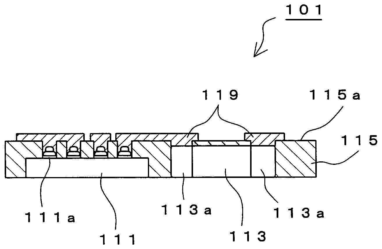
[0060]A manufacturing method for the electronic component-mounted component 101 will be described in the first place.

[0061]A process of mounting the semiconductor element 111 and the passive element 113 as electronic components into the base 115 includes a process of embedding the electronic components in the sheet-shaped base 115, a process of exposing electrodes 112 and 113a of the electronic components from the base 115, and a process of forming the circuit pattern 119 electrically connectible to the exposed electrodes 112 and 113a. The description here exemplifies the case of forming a sheet module having the semiconductor element 111 and the passive element 113 embedded in a thermoplastic sheet base as an example of the base 115.

[0062]The thermoplastic sheet base 115 is preferably, for example, polyethylene terephthalate, polyvinyl chloride, polycarbonate, acrylonitrile butadiene styrene, thermoplastic polyimide or the like having electrical insulating properties with a thickne...

second embodiment

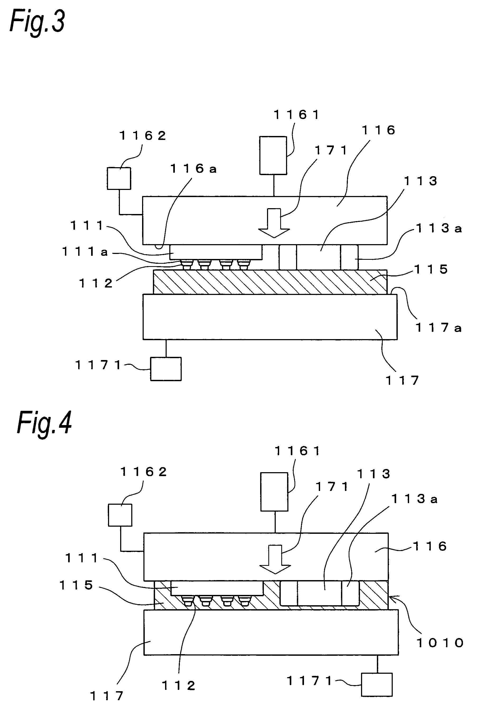
[0081]FIG. 7 shows a sheet module corresponding to the electronic component-mounted component 102 which has a through hole 118 penetrating the machining face 115a of the thermoplastic sheet base 115 and a rear face 115d opposite to the machining face 115a, and also a thin film capacitor 120 as contrasted with the electronic component-mounted component 101 shown in FIG. 1. The through hole 118 is formed by boring the thermoplastic sheet base 115 in its thickness direction by a laser, an ion beam or an electron beam. An inner peripheral face or inside of the through hole 118 is provided with a conductive material concurrently when the circuit pattern 119 is formed. Accordingly, an electric connection between the machining face 115a and the rear face 115d is obtained via the through hole 118 by at least one treatment of conductive sputtering, vapor deposition, filling a conductive material, and the like. A diameter of the through hole 118 is made, for instance, 0.1 mm. The thin film ca...

third embodiment

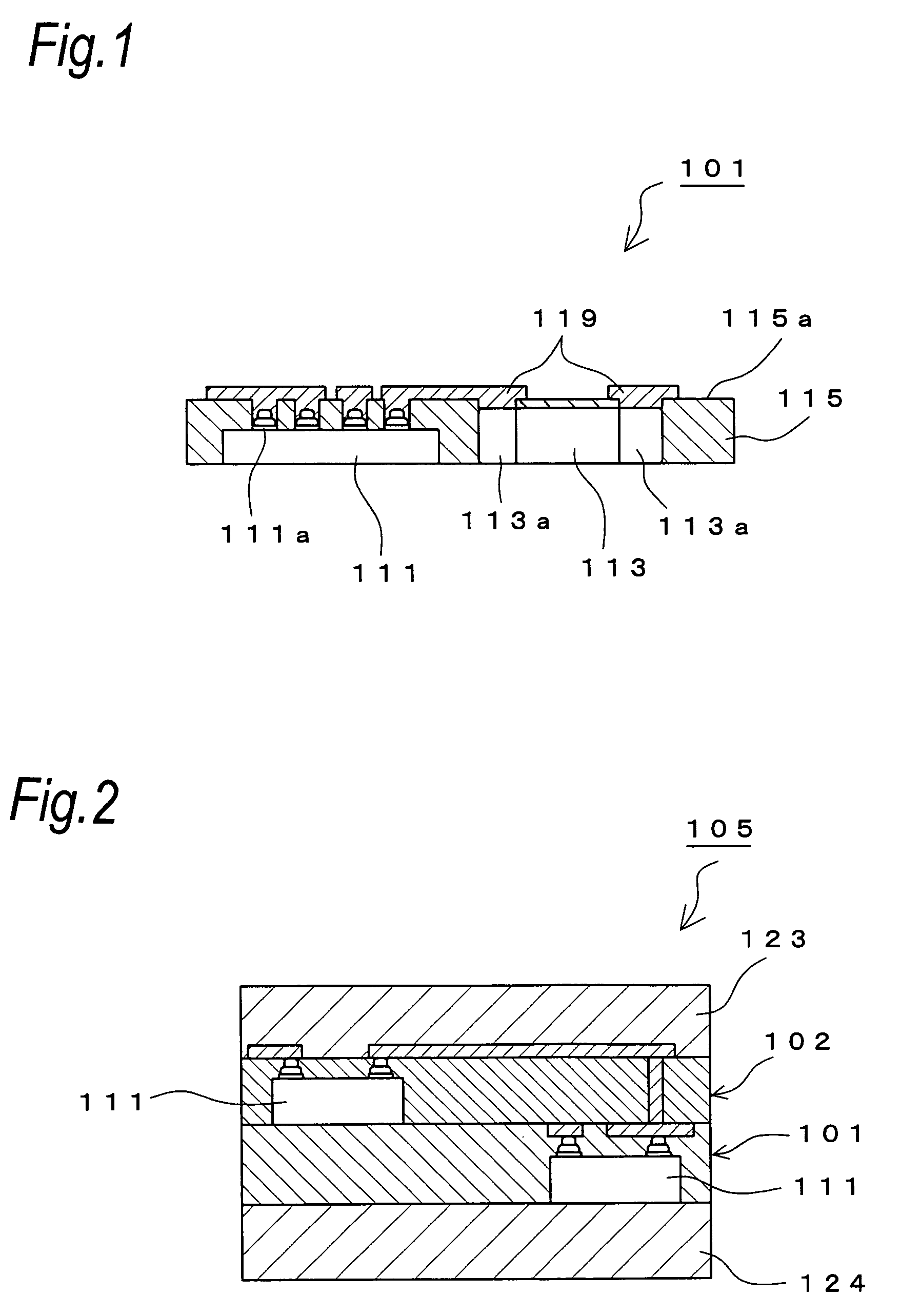
[0084]The electronic component-mounted component 101 in the above first embodiment and the electronic component-mounted component 102 in the above second embodiment are stacked in the thickness direction thereof and moreover laminated by two sheet-shaped protecting materials 123 and 124 to cover the electronic component-mounted components 101 and 102, whereby the electronic component-mounted completed product 105 as shown in FIG. 2 can be manufactured. The electronic component-mounted-component 102 included in the electronic component-mounted completed product 105 of this third embodiment has no circuit pattern 119 formed at the rear face 115d. The electronic component-mounted component 101 and the electronic component-mounted component 102 are registered with each other so that the through hole 118 formed in the electronic component-mounted component 102 is electrically connected to the circuit pattern 119 of the electronic component-mounted component 101. The electronic component-...


PUM

PropertyMeasurementUnit
glass transition pointaaaaaaaaaa
temperatureaaaaaaaaaa
glass transition pointaaaaaaaaaa

Abstract

A semiconductor element (111) with electrodes (112), and a passive element (113) with electrodes (113a) are embedded in a thermoplastic sheet base (115), which is then subjected to laser beam machining, electron beam machining or ion beam machining to expose electrodes (112 and 113a). Thereafter, a circuit pattern (119) is formed by formation of a thin film or printing of a conductive adhesive. Exposing the electrodes by laser beam machining or the like can be carried out in a short period of time and also by local treatment, thereby reducing damage to the base.

Description

BACKGROUND OF THE INVENTION[0001]The present invention relates to a manufacturing method for electronic component-mounted components to manufacture electronic component-mounted components by mounting electronic components such as semiconductor elements to a base, a manufacturing method for electronic component-mounted completed products with the electronic component-mounted components, and electronic component-mounted completed products with the electronic component-mounted components. The electronic component-mounted completed product with the electronic component-mounted components corresponds to stack modules, memory cards, non-contact IC cards and the like.[0002]A conventional manufacturing method for an electronic component-mounted completed product which has, for example, a plurality of semiconductor elements, capacitors, resistors and the like passive components mounted on one carrier substrate will be described below with reference to FIGS. 11 and 12.[0003]Conventionally, in...

Claims


Application Information

Patent Timeline
Patent Type & Authority Patents(United States)
IPC IPC(8): H01L21/44H05K1/16G06K19/077H01L21/56H01L21/60H01L23/12H01L23/498H01L23/538H01L25/00H05K1/18H05K3/46
CPCH01L23/49855H01L24/24H01L24/82H01L24/97H05K1/185Y10T29/49155H01L2224/24195H01L2224/24226H01L2224/73204H01L2224/97H01L2924/01004H01L2924/01013H01L2924/01018H01L2924/01029H01L2924/01033H01L2924/01039H01L2924/01046H01L2924/01047H01L2924/01074H01L2924/01078H01L2924/01079H01L2924/09701H01L2924/19041H01L2924/19043H01L2924/19105H01L23/5389H01L2924/07811H01L2924/014H01L2924/01072H01L2924/01024H01L2924/01019H01L2924/01006H01L2224/82H01L2924/00H01L21/568H01L2924/12042H01L2924/18162
Inventor SAKURAI, DAISUKETSUKAHARA, NORIHITO
Owner PANASONIC CORP
Why Eureka
Try Eureka