

Method for processing copper-graphene composite nanometer pattern through electron beams
A technology of graphene compounding and electron beam processing, which is applied in nanotechnology, photosensitive material processing, photolithographic exposure devices, etc., can solve the problems of no ultra-small-scale nanocomposite material patterning, high processing cost, and harsh processing conditions. , to achieve excellent mechanical properties and electrical and thermal conductivity, reduce production costs, and reduce the effects of processing procedures
- Summary
- Abstract
- Description
- Claims
- Application Information
AI Technical Summary
Problems solved by technology
Method used
Image

Examples
specific Embodiment
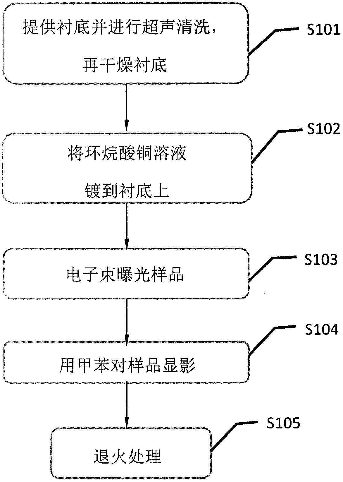
[0038] (1) S101 provides the substrate and performs ultrasonic cleaning and drying: select a single crystal silicon substrate, and ultrasonically clean it with acetone for 5 minutes, then ultrasonically clean it with isopropanol for 5 minutes, and then dry the sample with nitrogen;
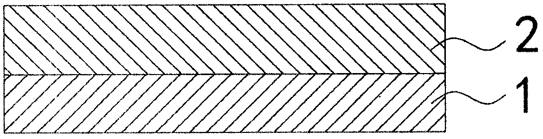
[0039] (2) S102 Copper naphthenate is plated on the substrate: first drop the copper naphthenate solution on the substrate and spin-coat with 1000 revolutions / second for 5 seconds and then spin-coat with 4000 revolutions / second for 60 seconds, the result Schematic such as figure 2 shown.
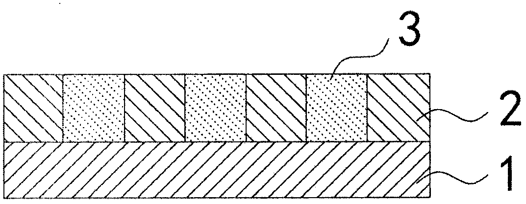
[0040] (3) S103 electron beam exposure sample: Use the electron beam exposure equipment Raith 150-Two to expose the sample in step 2. During the exposure process, the high voltage of the equipment is 30KV, and the beam current is 200PA; the schematic diagram of the result is as follows image 3 shown.
[0041] (4) S104 develops the sample with toluene: develop the exposed sample in a toluene solution for 60 s...
PUM
| Property | Measurement | Unit |
|---|---|---|
| Thickness | aaaaa | aaaaa |
Abstract
Description
Claims
Application Information