
Method for manufacturing film resistance

A technology of thin film resistors and manufacturing methods, applied to resistors, non-adjustable metal resistors, circuits, etc., can solve problems such as defective products, incomplete removal, and contamination by fine dust, so as to improve the yield rate and stabilize the characteristics of the resistive film , The effect of simplifying the manufacturing process

Inactive Publication Date: 2005-02-16
TA I TECH
View PDF0 Cites 11 Cited by
  • Summary
  • Abstract
  • Description
  • Claims
  • Application Information

AI Technical Summary

Problems solved by technology

However, when removing the photoresist, it may happen that the removal is incomplete, part of the resistive film is accidentally removed after removal, and after the photoresist film is removed, the resistive film is exposed to the normal room environment and is polluted by fine dust or partially oxidized. The electrical characteristics of thin film resistors may change as a result, and even lead to defective products

Method used


Image

  • Method for manufacturing film resistance
  • Method for manufacturing film resistance
  • Method for manufacturing film resistance

Examples


Embodiment Construction

[0027] In the following embodiments, a single thin-film resistor is chosen for illustration, but those skilled in the art will know that a plurality of thin-film resistors arranged in a matrix can be formed on a large insulating substrate during actual manufacturing.

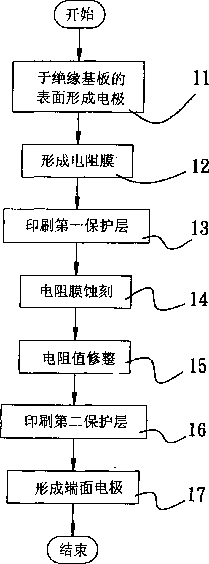
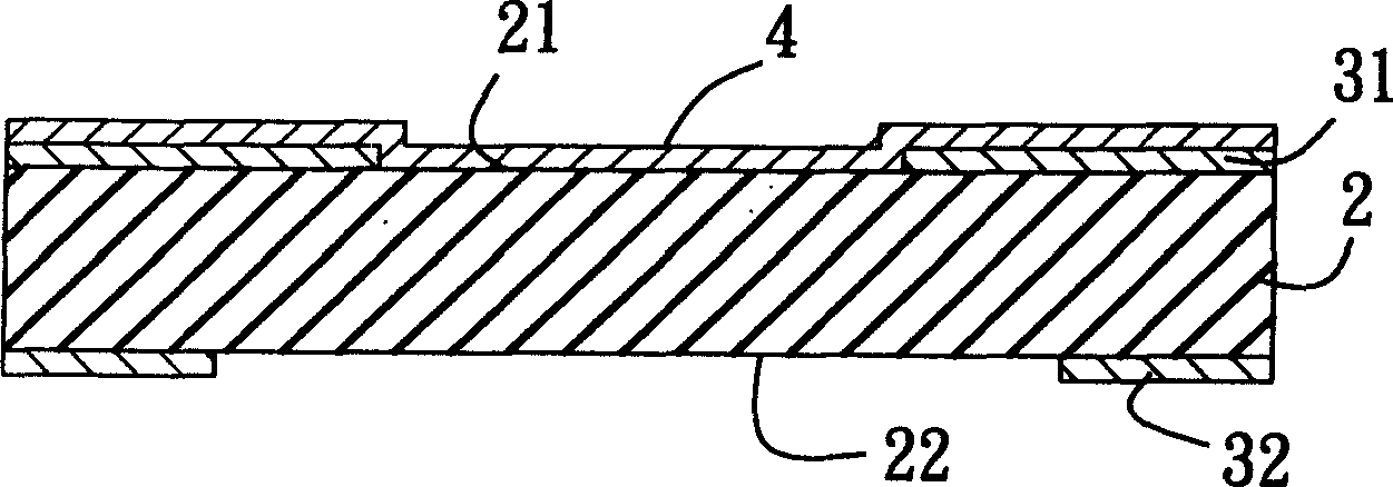
[0028] refer to figure 1 , the manufacturing process of a preferred embodiment of the manufacturing method of the thin film resistor of the present invention. In order to make this embodiment easier to understand, the following will cooperate Figure 2 to Figure 9 The manufacturing process of this embodiment will be described.

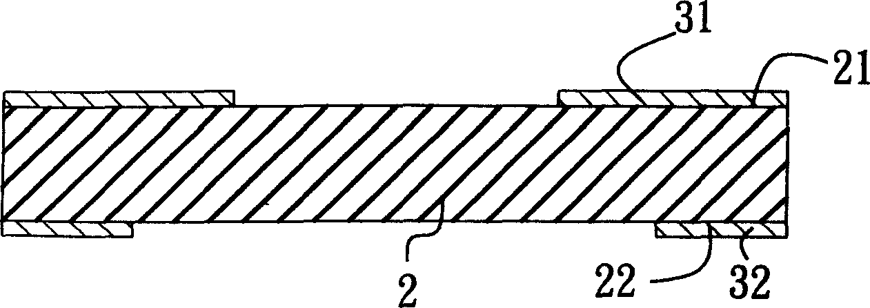
[0029] Firstly, step 11 is to form electrodes on the surface of an insulating substrate 2 . Such as figure 2 , two main electrodes 31 are respectively formed on two ends of the upper surface 21 of the insulating substrate 2 . In addition, in this embodiment, two bottom electrodes 32 can be formed on both ends of the bottom surface 22 of the insulating substrate 2 for bonding on a pr...


PUM


Abstract

First protection layer as a mask for etching resistance film further in order to form a patterned resistance film is formed on a resistance film through printing technique. The first protection layer can be utilized to protect resistance film, and does not need to be removed in following procedures. Thus, the invention simplifies fabricating flow and raises fineness rate of film resistor.

Description

technical field [0001] The present invention relates to a method for manufacturing a thin film resistor, in particular to a method for manufacturing a thin film resistor using a protective layer that does not need to be removed as a mask to define a resistive film pattern. Background technique [0002] Resistors can be divided into coil resistors and non-coil resistors. Non-coil resistors (chip resistors) are currently the most popular in the industry due to their small size, light weight, low cost, wide range of parameters, and wide applicability. The most used resistance element. Chip resistors can be divided into thin film resistors and thick film resistors according to the manufacturing method. [0003] As disclosed in Taiwan Patent No. 86113162, the resistive film of a thick film resistor is printed on a ceramic substrate using a screen frame, and then dried and sintered at a high temperature (such as 900° C.). The thickness of the resistive film is about 5 to 10 μm a...

Claims


Application Information

Patent Timeline
IPC IPC(8): H01C7/00H05K3/30
Inventor 蔡承琪陈文生庄弘毅江财宝
Owner TA I TECH
Learn More