Optical mask, method for making figure and method for making semiconductor device

A mask pattern and photomask technology, which is applied in the field of photolithography, can solve the problems that it is difficult to set up dummy patterns, it is difficult to planarize the interlayer dielectric film, and it is impossible to form photoresist patterns.

A mask pattern and photomask technology, which is applied in the field of photolithography, can solve the problems that it is difficult to set up dummy patterns, it is difficult to planarize the interlayer dielectric film, and it is impossible to form photoresist patterns.

CN1581437AInactive Publication Date: 2005-02-16KK TOSHIBA

Image

  • Optical mask, method for making figure and method for making semiconductor device
  • Optical mask, method for making figure and method for making semiconductor device
  • Optical mask, method for making figure and method for making semiconductor device

Examples


Embodiment Construction

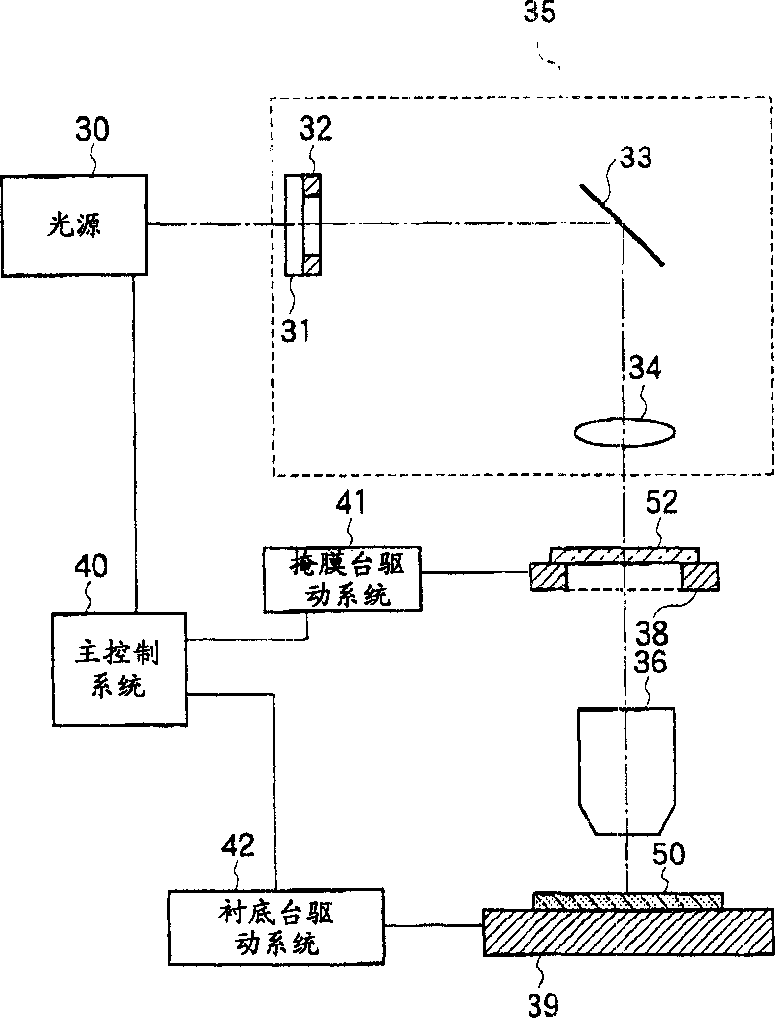
[0023] Embodiments of the present invention will be described below with reference to the drawings. Note that throughout the drawings, the same or similar reference numerals denote the same or similar parts and units, and descriptions of the same or similar parts and units will be omitted or simplified.

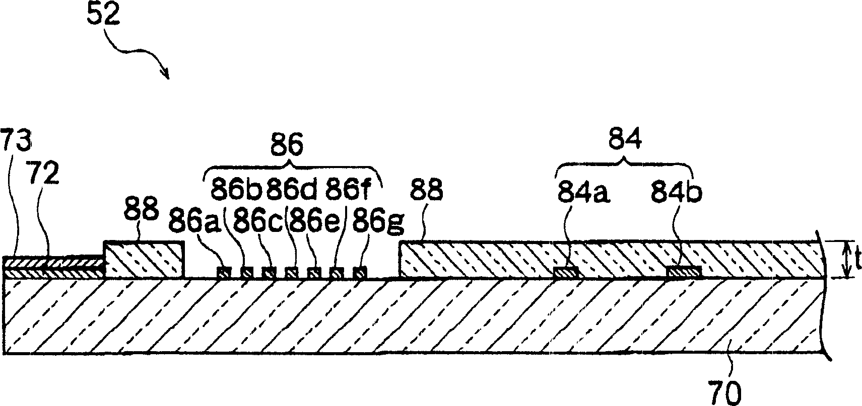
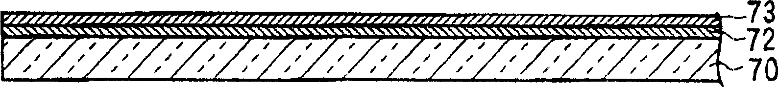
[0024] Such as figure 1 As shown, a photomask 52 according to an embodiment of the present invention includes a transparent substrate 70 , a first mask pattern 84 , a second mask pattern 86 and a transparent film 88 . First and second mask patterns 84, 86 are provided on the transparent substrate 70, and a transparent film 88 having an actual film thickness t is located in the pattern area including the mask pattern 84 provided therein. For the first mask pattern 84, in figure 1 The cross-sectional view of the first mask portion 84a, 84b is shown, and for the second mask pattern 86, in figure 1 The second mask portions 86a to 86g are shown in the cross-sectional view of . ...


PUM

PropertyMeasurementUnit
thicknessaaaaaaaaaa
thicknessaaaaaaaaaa
refractive indexaaaaaaaaaa

Abstract

A photomask includes a transparent substrate; a first mask pattern disposed on a first region of the transparent substrate; a second mask pattern disposed on a second region different from the first region of the transparent substrate; and a transparent film provided on the first mask pattern, having an optical thickness configured to make a focal position of the first mask pattern deeper than a focal position of the second mask pattern.

Description

[0001] Cross References to Related Applications [0002] This application is based upon and claims priority from prior Japanese Patent Application P2003-289008 filed on Aug. 7, 2003, the entire contents of which are incorporated herein by reference. technical field [0003] The present invention relates to photolithography, and more particularly to a photomask, a method of making patterns using a photomask, and a method of manufacturing semiconductor devices. Background technique [0004] When forming a circuit pattern of a semiconductor device, a photosensitive material such as a photoresist is coated on a working film on a semiconductor substrate, and then the photosensitive material is exposed and developed using a reduced projection photolithography machine. When using a photolithography machine with a refractive optical system, the light emitted from the light source passes through the illumination optical system and the projection optical system, and the circuit patter...

Claims


Application Information

Patent Timeline
16 Feb 2005
Publication
CN1581437A
IPC
G03C5/00; G03F1/54; G03F1/56; G03F7/16; G03F7/20; G03F9/00; G03G16/00; H01L21/00; H01L21/027
CPC
G03F1/144; G03F1/70
Inventors
δΌŠθ—€δ»