Liquid crystal display and its mfg method

A liquid crystal display device, liquid crystal technology, applied in semiconductor/solid-state device manufacturing, static indicators, optics, etc.

Inactive Publication Date: 2005-03-09
QUANTA DISPLAY +1
View PDF3 Cites 5 Cited by
  • Summary
  • Abstract
  • Description
  • Claims
  • Application Information

AI Technical Summary

Problems solved by technology

However, in the current situation, the channel length, that is, the pattern size of the halftone exposure area, is affected by the exposure amount (the pattern accuracy of the light source intensity and the photomask, especially the line / space spacing size), the coating thickness of the photosensitive resin, and the photosensitive resin. Influenced by many parameters such as the development process of the etching process and the reduction of the thickness of the photosensitive resin film in the etching step, coupled with the in-plane uniformity of these quantities, it may not be possible to produce in a state of high yield and stability. There is more strict manufacturing management than in the past, so I dare not say that there will be high-level output

Method used


Image

  • Liquid crystal display and its mfg method
  • Liquid crystal display and its mfg method
  • Liquid crystal display and its mfg method

Examples


no. 1 Embodiment

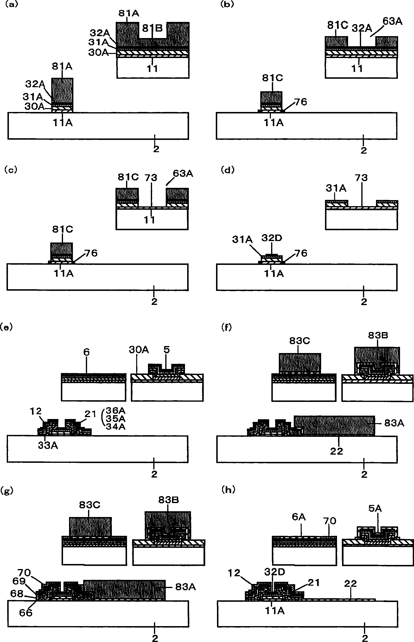
[0203] The first embodiment is the same as the conventional example. First, on one main surface of the glass substrate 2, a vacuum film forming device such as SPT is used to coat a film with a thickness of about 0.1 to 0.3 μm, such as Cr, Ta, Mo, or the like. These alloys or silicides are used as the first metal layer. As can be seen from the subsequent description, the present invention has almost no restrictions on the material of the scanning line when selecting an organic insulating layer for the insulating layer formed on the side of the gate insulating layer. However, for the insulating layer formed on the side of the gate insulating layer, select When the anodized film layer is used, the anodized layer must be insulating. At this time, if the high resistance of the Ta monomer and the lack of heat resistance of the Al monomer are taken into consideration, in order to achieve low resistance of the scanning line, The configuration of the scanning line must be selected from...

no. 2 Embodiment

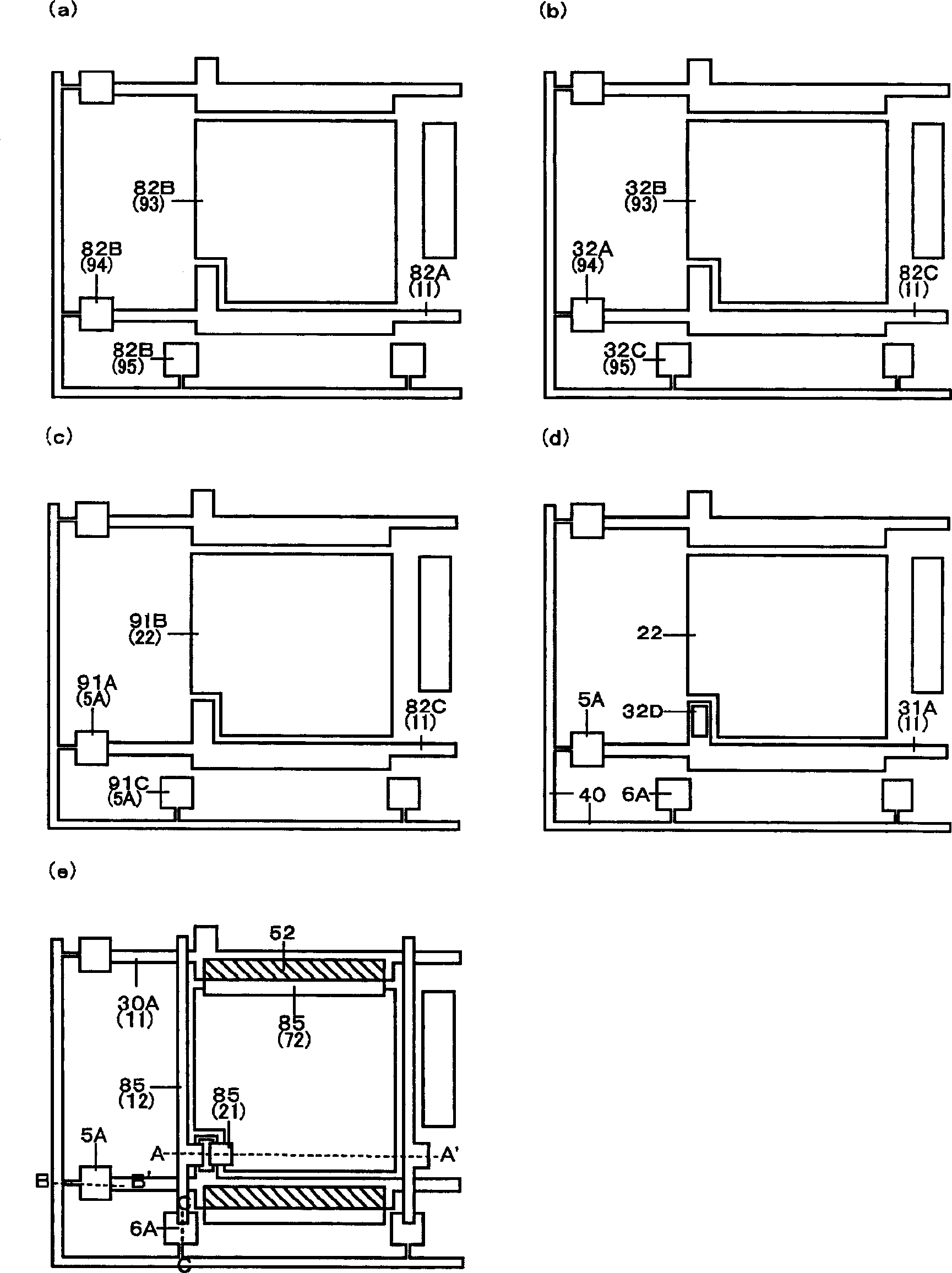
[0218] In the second embodiment, firstly, on one main surface of the glass substrate 2, use a vacuum film-forming device such as SPT to cover: a transparent conductive layer 91 with a film thickness of about 0.1 to 0.2 μm, such as ITO; and a film thickness of 0.1 to 0.2 μm. The transparent conductive layer 91 is about 0.2 μm; and the first metal layer 92 is about 0.1 to 0.3 μm in thickness. It can be seen from the following description that in the second to fourth embodiments, the scan lines are laminated with transparent conductive layers and metal layers, so anodic oxidation cannot be used to form an insulating layer on the side of the scan lines. Here, because the organic insulating layer is formed on the insulating layer by electroplating, as far as the scanning line material is concerned, the first metal layer that does not react with ITO as the transparent conductive layer can be selected, such as Cr, Ta, Mo, etc. Refractory metals or alloys or silicides of these. To ac...

no. 3 Embodiment

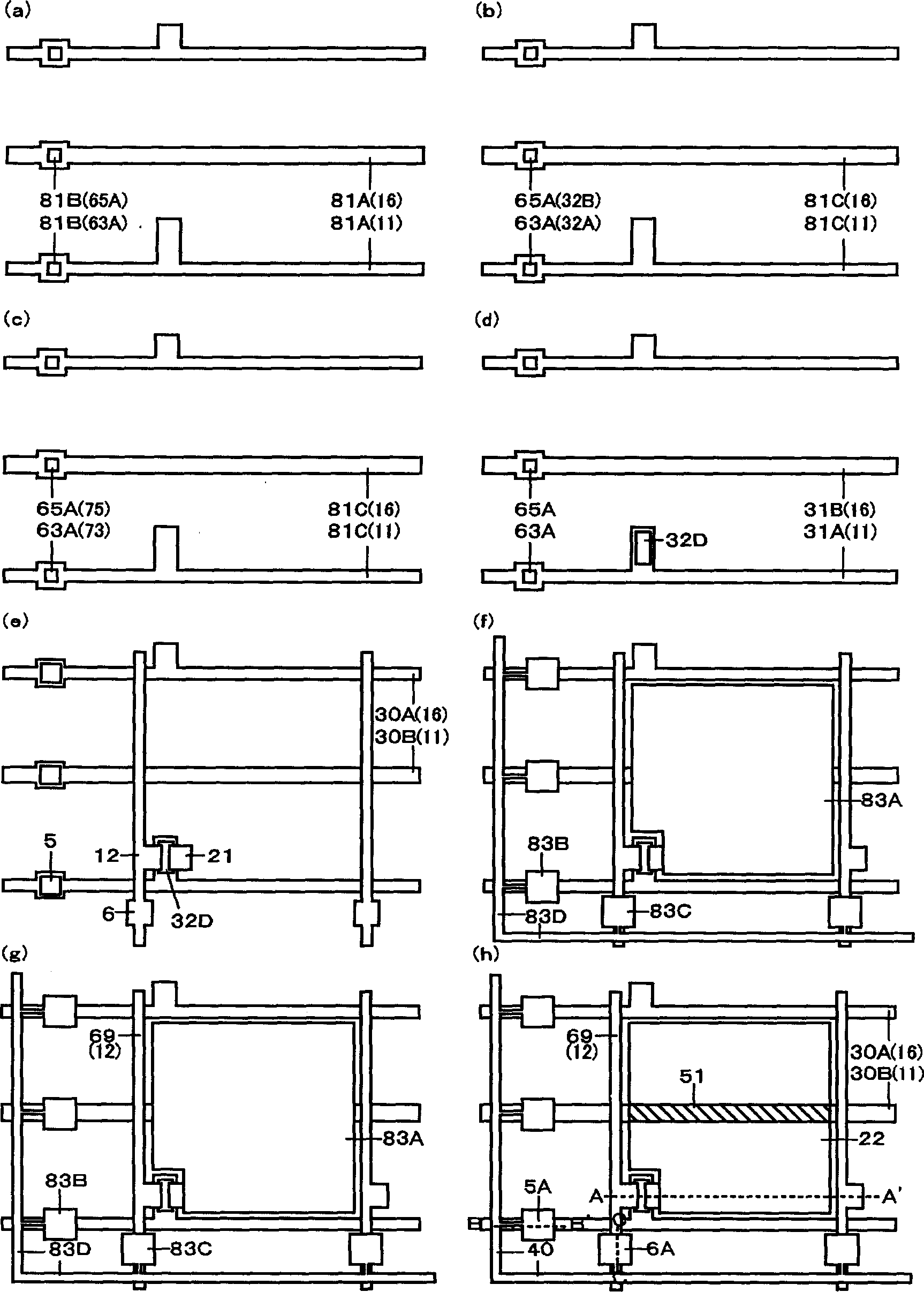
[0228] The third embodiment is as Figure 5 (d) and Figure 6 As shown in (d), the steps up to the formation step of the etching stopper layer 32D are substantially the same as those in the second embodiment. However, the dummy electrode terminal 95 is not necessarily required for reasons described later. Next, in the step of forming the source / drain wiring, use a vacuum film forming device such as SPT to sequentially cover: a thin film layer 34 such as Ti and Ta with a film thickness of about 0.1 μm as a heat-resistant metal layer; and a film thickness of 0.3 μm. The left and right AL thin film layers 35 serve as low-resistance wiring layers. Using the photosensitive resin pattern 86 using microfabrication technology, the source / drain wiring material, the second amorphous silicon layer 33, and the first amorphous silicon layer 31A composed of these two thin films are sequentially etched, and The gate insulating layer 30A is exposed. Such as Figure 5 (e) and FIG. 46 (e),...


PUM

PropertyMeasurementUnit
thicknessaaaaaaaaaa
thicknessaaaaaaaaaa
thicknessaaaaaaaaaa

Abstract

To solve the problem point that in the conventional manufacturing method decreased in the number of manufacturing stages, manufacture margin is small as a channel length becomes short and the the yield decreases. Four-mask process and three-mask process plans of a TN type liquid crystal display and an IPS type liquid crystal are structured by a technology combination of new technology for rationalizing a stage of forming scanning lines and a stage of forming contacts by introducing half-tone exposure technology, new technology for rationalizing a stage of forming the protective layer of an electrode terminal by introducing half-tone exposure technology into an anode oxidizing stage of source and drain wiring as known technology, and rationalization technology for forming pixel electrodes and the scanning lines at the same time as known technology.

Description

technical field [0001] The present invention relates to a liquid crystal display device with a color image display function, in particular to an active liquid crystal display device. Background technique [0002] In recent years, with the advancement of microfabrication technology, liquid crystal material technology and high-density mounting technology, among liquid crystal display devices with a diagonal of 5 to 50 cm, a large number of TV images or various image display devices are provided on a commercial basis. In addition, by pre-forming RGB colored layers on one side of the two glass substrates constituting the liquid crystal panel, it is relatively easy to realize color display. Especially in the so-called active liquid crystal panel in which switching elements are provided in each pixel, there is less cross-talk between signals, and the response speed is faster, so that an image with high contrast value can be obtained. [0003] Generally, these liquid crystal displ...

Claims


Application Information

Patent Timeline
Patent Type & Authority Applications(China)
IPC IPC(8): G02F1/1335G02F1/133G02F1/136G02F1/1368H01L21/00
Inventor 川崎清弘
Owner QUANTA DISPLAY
Why Eureka
Try Eureka